- 您現(xiàn)在的位置:買賣IC網(wǎng) > PDF目錄374016 > ADM8840 (Analog Devices, Inc.) Charge Pump Regulator & COM Driver for Color TFT Panel PDF資料下載
參數(shù)資料
| 型號: | ADM8840 |
| 廠商: | Analog Devices, Inc. |
| 英文描述: | Charge Pump Regulator & COM Driver for Color TFT Panel |
| 中文描述: | 電荷泵穩(wěn)壓器 |
| 文件頁數(shù): | 7/10頁 |
| 文件大小: | 166K |
| 代理商: | ADM8840 |
ADM8840
–
7
–
REV. PrG
2/03
PRELIMINARY TECHNICAL DATA
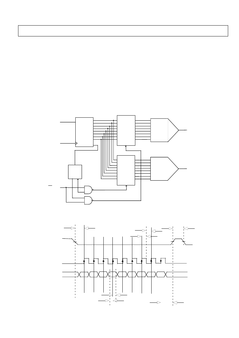
SERIAL INTERFACE
The COM Driver section of the ADM8840 uses a serial
interface to input data and transfer it into the DACs. Figure
3, below, shows the operation of the serial interface. The data
is transmitted along the serial DATA line, along with a serial
clock signal, SCLK. This data is read into a Shift Register.
When the 8 bits are sucessfully stored in the Shift Register a
low-to-high transition on the CS/LDAC input causes the
latch to load the 8-bits of data into the relevent DAC.
This function is also shown in the waveforms in Figure 4
below. A falling edge on the CS/LDAC input initiates the
data read into the shift register. The first bit of the datastream
is the DAC Select Bit (DAC_SEL) which determines which
internal DAC the data will be written to. A ‘1’ selects DAC
1 which sets the Amplitude of the output and a ‘0’ selects
Figure 4. Serial Interface Waveforms
t
4
D7
t
3
D2
D3
D4
D5
D6
t
5
t
7
t
6
CS /
LDAC
DATA
SCLK
t
1
t
2
D0
D1
DAC
SEL
SHIFT
REGISTER
SCLK
DATA
DAC1
LATCH
CS/LDAC
8 DATABITS
DAC2
LATCH
DAC
SELECT
DAC_SEL BIT
DAC 1 OUT
DAC2 OUT
DAC1
(AMPLITUDE)
DAC2
(CENTRE VOLTAGE)
Figure 3. Serial Interface Diagram
DAC 2 which sets the Centre Voltage of the output. The
individual data bits are then read in one by one on the DATA
line. After the DAC_SEL bit and the 8 data bits have been
read there is a pause to ensure the shift register outputs are
stable. Then a rising edge on the CS/LDAC input loads the
8 bits on the shift register outputs into the relevent DAC (and
the DAC outputs will change accordingly). Note that if CS/
LDAC goes high before all 8 data bits are read in then
incorrect data will be loaded into the DACs. All bits on the
DATA line are read in on each rising edge of the SCLK
signal.
When the ADM8840 comes out of shutdown the DACs
are preset with default values generating a COM_OUT
Amplitude of 6V with a Centre voltage of 1.5V.
相關(guān)PDF資料 |
PDF描述 |
|---|---|
| ADM8840ACP | 20-17 (6 Contacts) Socket Insert; For Use With:Amphenol MIL-C-5015 97 Series Circular Connectors; No. of Contacts:6 |
| ADM8845 | Charge Pump Driver for LCD White LED Backlights |
| ADM8845ACP | Charge Pump Driver for LCD White LED Backlights |
| ADM8845ACP-REEL7 | Charge Pump Driver for LCD White LED Backlights |
| ADM8845ACPZ | Charge Pump Driver for LCD White LED Backlights |
相關(guān)代理商/技術(shù)參數(shù) |
參數(shù)描述 |
|---|---|
| ADM8840ACP | 制造商:Analog Devices 功能描述:LCD DRVR 2.7V TO 3.6V 32LFCSP - Bulk |
| ADM8840ACP-REEL7 | 制造商:Analog Devices 功能描述: |
| ADM8843 | 制造商:AD 制造商全稱:Analog Devices 功能描述:4 White LED Backlight Driver |
| ADM8843ACPZ | 制造商:Analog Devices 功能描述:LED DRVR 4SEGMENT 3.3V/5V 16LFCSP EP - Bulk |
| ADM8843ACPZ1-R7 | 制造商:Analog Devices 功能描述: |
發(fā)布緊急采購,3分鐘左右您將得到回復(fù)。