- 您現(xiàn)在的位置:買賣IC網(wǎng) > PDF目錄373994 > ADL5390ACPZ-WP1 (Analog Devices, Inc.) RF/IF Vector Multiplier PDF資料下載
參數(shù)資料
| 型號(hào): | ADL5390ACPZ-WP1 |
| 廠商: | Analog Devices, Inc. |
| 英文描述: | RF/IF Vector Multiplier |
| 中文描述: | 射頻中頻向量乘法器/ |
| 文件頁(yè)數(shù): | 16/24頁(yè) |
| 文件大?。?/td> | 716K |
| 代理商: | ADL5390ACPZ-WP1 |
第1頁(yè)第2頁(yè)第3頁(yè)第4頁(yè)第5頁(yè)第6頁(yè)第7頁(yè)第8頁(yè)第9頁(yè)第10頁(yè)第11頁(yè)第12頁(yè)第13頁(yè)第14頁(yè)第15頁(yè)當(dāng)前第16頁(yè)第17頁(yè)第18頁(yè)第19頁(yè)第20頁(yè)第21頁(yè)第22頁(yè)第23頁(yè)第24頁(yè)
ADL5390
3GPP2 C.S0010-B, Table 6.5.2.1) was applied to the ADL5390.
A cavity-tuned filter was used to reduce noise from the signal
source being applied to the device. The 4.6 MHz pass band of
this filter is apparent in the subsequent spectral plots.
Rev. 0 | Page 16 of 24
Figure 35 shows the output signal spectrum for a programmed
gain and phase of 5 dB and 45
o
. P
OUT
is equal to 0 dBm and
V
IBB
= V
QBB
= 0.353 V (centered around 500 mV), i.e., V
IBBP
V
IBBM
= V
QBBP
V
QBBM
= 0.353 V. Adjacent channel power is
measured in 30 kHz resolution bandwidth at 750 kHz and
1.98 MHz carrier offset. Noise floor is measured at ±4 MHz
carrier offset in a 1 MHz resolution bandwidth.
1
CU2
CU1
CU1
C0
C0
Cl1
Cl1
Cl2
Cl2
0
A
CENTER 880MHz
500kHz/
SPAN 5MHz
REF LVL
1AVG
MARKER 1 [T1]
RBW 30kHz
RF ATT
20dB
dB
1 [T1] –1CH PWR
0
–70
–80
–90
–100
–60
–50
–40
–30
–20
–10
1 [T1]
0.13dBm
1RM
EXT
Figure 35. Output Spectrum, Single-Carrier CDMA2000 Test Model at 5 dBm,
V
I
= V
Q
= 0.353 V, ACP Measured at 750 kHz and 1.98 MHz Carrier Offset,
Input Signal–Filtered Using a Cavity-Tuned Filter (Pass Band = 4.6 MHz)
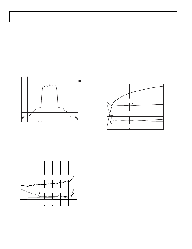
Holding the I and Q gain control voltages steady at 0.353 V,
input power was swept. Figure 36 shows the resulting output
power, noise floor, and adjacent channel power ratio. The noise
floor is presented as noise in a 1 MHz bandwidth as defined by
the 3GPP2 specification.
–30
–100
–90
–80
–70
–60
–50
–40
–30
–100
–90
–80
–70
–60
–50
–40
–30
–25
–20
–15
–10
–5
0
5
0
OUTPUT POWER (dBm)
A
N
ACP: 750kHz OFFSET, 30kHz RBW
ACP: 1.98MHz OFFSET, 30kHz RBW
NOISE: 4MHz OFFSET, 1MHz RBW
Figure 36. Noise and ACP vs. Output Power, Single-Carrier CDMA2000 Test
Model, V
I
= V
Q
= 0.353, ACP Measured in 30 kHz RBW at ±750 kHz and
±1.98 MHz Carrier Offset, Noise Measured at ±4 MHz Carrier Offset
ACP is still in compliance with the standard (<45 dBc @
750 kHz and <60 dBc @ 1.98 MHz) even with output powers
greater than +3 dBm. At low output power levels, ACP at
1.98 MHz carrier offset degrades as the noise floor of the
ADL5390 becomes the dominant contributor to measured ACP.
Measured noise at 4 MHz carrier offset begins to increase
sharply above 2 dBm output power. This increase is not due to
noise, but results from increased carrier-induced distortion. As
output power drops below 2 dBm, the noise floor drops towards
90 dBm.
With a fixed input power of 2.16 dBm, the output power was
again swept by changing V
IBB
and V
QBB
from 0 V to 500 mV.
The resulting output power, ACP, and noise floor are shown in
Figure 37.
5
–44
–37
–30
–23
–16
–9
–2
–30
–100
0.5
–90
–80
–70
–60
–50
–40
0
0.1
0.2
0.3
0.4
0
V
I(Q)BB
R
N
A
V
OUT
vs. V
IBB
/V
QBB
ACP: 750kHz OFFSET, 30kHz RBW
NOISE: 4MHz OFFSET, 1MHz RBW
ACP: 1.98MHz OFFSET, 30kHz RBW
Figure 37. Output Power, Noise, and ACP vs. I and Q Control Voltages,
CDMA2000 Test Model, V
I
= V
Q
, ACP Measured in 30 kHz RBW at ±750 MHz
and ±1.98 MHz Carrier Offset, Noise Measured at ±4 MHz Carrier Offset
In contrast to Figure 36, Figure 37 shows that for a fixed input
power, ACP remains fairly constant as gain and phase are
changed (this is not true for very high RF input powers) until
the noise floor of the ADL5390 becomes the dominant con-
tributor to the measured ACP.
相關(guān)PDF資料 |
PDF描述 |
|---|---|
| ADL5390 | RF/IF Vector Multiplier |
| ADL5391 | DC to 2.0 GHz Multiplier |
| ADL5391ACPZ-R2 | DC to 2.0 GHz Multiplier |
| ADL5391ACPZ-R7 | DC to 2.0 GHz Multiplier |
| ADL5391ACPZ-WP | DC to 2.0 GHz Multiplier |
相關(guān)代理商/技術(shù)參數(shù) |
參數(shù)描述 |
|---|---|
| ADL5390-EVAL | 制造商:Analog Devices 功能描述:EVALUATION BOARD FOR RF/IF VECTOR MULTIPLIER 制造商:Analog Devices 功能描述:EVALUATION BOARD FOR ADL5390 - Bulk |
| ADL5390-EVALZ | 制造商:Analog Devices 功能描述:Evaluation Board For ADL5390 制造商:Analog Devices 功能描述:EVALUATION BOARDS - Bulk |
| ADL5391 | 制造商:AD 制造商全稱:Analog Devices 功能描述:DC to 2.0 GHz Multiplier |
| ADL5391ACPZ | 制造商:Analog Devices 功能描述:IC, MULTIPLIER, 2.0GHZ, 16LFCSP 制造商:Analog Devices 功能描述:IC, MULTIPLIER, 2.0GHZ, 16LFCSP; IC Function:Analogue Multiplier; Brief Features:3 dB bandwidth of 2 GHz; Supply Voltage Min:4.5V; Supply Voltage Max:5.5V; Operating Temperature Min:-40C; Operating Temperature Max:85C; Digital IC ;RoHS Compliant: Yes |
| ADL5391ACPZ-R2 | 制造商:Analog Devices 功能描述:DC TO 2.0 GHZ MULTIPLIER - Tape and Reel |
發(fā)布緊急采購(gòu),3分鐘左右您將得到回復(fù)。