- 您現(xiàn)在的位置:買賣IC網(wǎng) > PDF目錄165349 > ADL5306ACPZ-R2 (ANALOG DEVICES INC) SPECIALTY ANALOG CIRCUIT, QCC16 PDF資料下載
參數(shù)資料
| 型號: | ADL5306ACPZ-R2 |
| 廠商: | ANALOG DEVICES INC |
| 元件分類: | 模擬信號調(diào)理 |
| 英文描述: | SPECIALTY ANALOG CIRCUIT, QCC16 |
| 封裝: | 3 X 3 MM, MO-220VEED-2, LFCSP-16 |
| 文件頁數(shù): | 3/16頁 |
| 文件大小: | 1015K |
| 代理商: | ADL5306ACPZ-R2 |
ADL5306
Rev. 0 | Page 11 of 16
APPLICATIONS
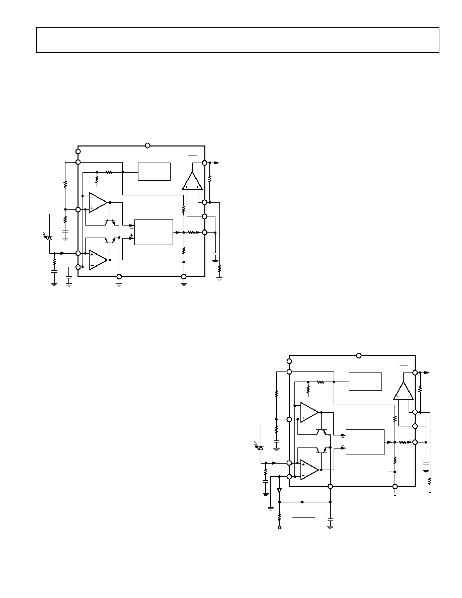
The ADL5306 is easy to use in optical supervisory systems and
in similar situations where a wide-ranging current is to be
converted to its logarithmic equivalent (i.e., represented in
decibel terms). Basic connections for measuring a single current
input are shown in Figure 22, which includes various
nonessential components, as will be explained.
TEMPERATURE
COMPENSATION
BIAS
GENERATOR
451
8k
12k
14.2k
80k
20k
RREF
200k
6.69k
COMM
VNEG
VSUM
VPOS
INPT
VREF
NC
IREF
0.5V
+5V
2.5V
0.5V
VBE1
ILOG
VBE2
VOUT
SCAL
BFIN
VLOG
0.5 log10
( )
IPD
1nA
1k
1k
1nF
VBIAS
IPD
Q2
Q1
CFLT
10nF
03727-0-022
Figure 22. Basic Connections for Fixed Intercept Use
The 2 V difference in voltage between VREF and INPT, in
conjunction with the external 200 k resistor RREF, provides a
reference current IREF of 100 A into Pin IREF. The internal
reference raises the voltage at VLOG by 0.8 V, effectively
lowering the intercept current IINTC by a factor of 104 to position
it at 1 nA. Any temperature variation in RREF must be taken into
account when estimating the stability of the intercept. Also, the
overall noise will increase when using very low values of IREF. In
fixed-intercept applications, there is little benefit in using a large
reference current, since this only compresses the low current
end of the dynamic range when operated from a single supply,
shown here as 5 V. The capacitor between VSUM and ground is
recommended to minimize the noise on this node and to help
provide a clean reference current.
Since the basic scaling at VLOG is 0.2 V/dec and a swing of 4 V
at the buffer output would therefore correspond to 20 decades,
it will often be useful to raise the slope to make better use of the
rail-to-rail voltage range. For illustrative purposes, the circuit in
Figure 22 provides an overall slope of 0.5 V/dec (25 mV/dB).
Thus, using IREF = 100 A, VLOG runs from 0.2 V at IPD = 100 nA
to 0.8 V at IPD = 100 A. The buffer output runs from 0.5 V to
2.0 V, corresponding to a dynamic range of 60 dB electrical
(30 dB optical) power.
The optional capacitor from VLOG to ground forms a single-
pole low-pass filter in combination with the 4.55 k resistance
at this pin. For example, using a CFLT of 10 nF, the –3 dB corner
frequency is 3.2 kHz. Such filtering is useful in minimizing the
output noise, particularly when IPD is small. Multipole filters are
more effective in reducing the total noise. For examples, see the
AD8304 Data Sheet.
The dynamic response of this overall input system is influenced
by the external RC networks connected from the two inputs
(INPT, IREF) to ground. These are required to stabilize the
input systems over the full current range. The bandwidth
changes with the input current due to the widely varying pole
frequency. The RC network adds a zero to the input system to
ensure stability over the full range of input current levels. The
network values shown in Figure 22 will usually suffice, but some
experimentation may be necessary when the photodiode’s
capacitance is high.
Although the two current inputs are similar, some care is
needed to operate the reference input at extremes of current
(<100 nA) and temperature (<0°C). Modifying the RC network
to 4.7 nF and 2 kΩ will allow operation to –40°C at 10 nA. By
inspecting the transient response to perturbations in IREF at
representative current levels, the capacitor value can be adjusted
to provide fast rise and fall times with acceptable settling. To
fine-tune the network zero, the resistor value should be
adjusted.
USING A NEGATIVE SUPPLY
Most applications of the ADL5306 require only a single supply
of 3.0 V to 5.5 V. However, to provide further versatility, dual
supplies may be employed, as illustrated in Figure 23.
TEMPERATURE
COMPENSATION
BIAS
GENERATOR
451
8k
12k
14.2k
80k
20k
RREF
200k
6.69k
COMM
VNEG
VSUM – VF ≤ –0.5V
VF
RS ≤
Iq + Isig
Isig = IPD + IREF
VN
VSUM
VPOS
INPT
VREF
NC
IREF
0.5V
+5V
2.5V
0.5V
VBE1
ILOG
VBE2
VOUT
SCAL
BFIN
VLOG
0.5 log10
( )
IPD
1nA
1k
1k
1nF
VBIAS
IPD
Q2
Q1
CFLT
10nF
C1
VN – VF
Iq + Isigmax
03727-0-023
Figure 23. Negative Supply Application
相關(guān)PDF資料 |
PDF描述 |
|---|---|
| ADM1033ARQ-REEL | DIGITAL TEMP SENSOR-SERIAL, 8BIT(s), 2Cel, RECTANGULAR, SURFACE MOUNT |
| ADM1069AST | 8-CHANNEL POWER SUPPLY SUPPORT CKT, PQFP32 |
| ADM231LAN | 5V High-Speed RS-232 Transceivers with 0.1uF Capacitors |
| ADM231LAQ | 5V High-Speed RS-232 Transceivers with 0.1uF Capacitors |
| ADM231LAR | 5V High-Speed RS-232 Transceivers with 0.1uF Capacitors |
相關(guān)代理商/技術(shù)參數(shù) |
參數(shù)描述 |
|---|---|
| ADL5306ACPZ-REEL7 | 功能描述:IC CONV LOGARITHMIC 60DB 16LFCSP RoHS:是 類別:集成電路 (IC) >> 線性 - 放大器 - 專用 系列:- 產(chǎn)品培訓模塊:Lead (SnPb) Finish for COTS Obsolescence Mitigation Program 標準包裝:60 系列:- 類型:可變增益放大器 應(yīng)用:CATV 安裝類型:表面貼裝 封裝/外殼:20-WQFN 裸露焊盤 供應(yīng)商設(shè)備封裝:20-TQFN-EP(5x5) 包裝:托盤 |
| ADL5306-EVAL | 制造商:Analog Devices 功能描述:Evaluation Board For IC Log Amp Single 5.5V 制造商:Analog Devices 功能描述:LOG AMP SGL 5.5V - Bulk |
| ADL5310 | 制造商:AD 制造商全稱:Analog Devices 功能描述:120 dB Range (3 nA to 3 mA) Dual Logarithmic Converter |
| ADL5310ACP | 制造商:Rochester Electronics LLC 功能描述:LOGARITHMIC CONVERTER - Bulk |
| ADL5310ACP-R2 | 功能描述:IC LOGARITHMIC CONV DUAL 24LFCSP RoHS:否 類別:集成電路 (IC) >> 線性 - 放大器 - 專用 系列:- 產(chǎn)品培訓模塊:Lead (SnPb) Finish for COTS Obsolescence Mitigation Program 標準包裝:60 系列:- 類型:可變增益放大器 應(yīng)用:CATV 安裝類型:表面貼裝 封裝/外殼:20-WQFN 裸露焊盤 供應(yīng)商設(shè)備封裝:20-TQFN-EP(5x5) 包裝:托盤 |
發(fā)布緊急采購,3分鐘左右您將得到回復(fù)。