- 您現(xiàn)在的位置:買(mǎi)賣(mài)IC網(wǎng) > PDF目錄373980 > ADE7759 (Analog Devices, Inc.) Active Energy Metering IC with di/dt Sensor Interface PDF資料下載
參數(shù)資料
| 型號(hào): | ADE7759 |
| 廠(chǎng)商: | Analog Devices, Inc. |
| 英文描述: | Active Energy Metering IC with di/dt Sensor Interface |
| 中文描述: | 有源電能計(jì)量IC的di / dt傳感器接口 |
| 文件頁(yè)數(shù): | 29/32頁(yè) |
| 文件大小: | 530K |
| 代理商: | ADE7759 |
第1頁(yè)第2頁(yè)第3頁(yè)第4頁(yè)第5頁(yè)第6頁(yè)第7頁(yè)第8頁(yè)第9頁(yè)第10頁(yè)第11頁(yè)第12頁(yè)第13頁(yè)第14頁(yè)第15頁(yè)第16頁(yè)第17頁(yè)第18頁(yè)第19頁(yè)第20頁(yè)第21頁(yè)第22頁(yè)第23頁(yè)第24頁(yè)第25頁(yè)第26頁(yè)第27頁(yè)第28頁(yè)當(dāng)前第29頁(yè)第30頁(yè)第31頁(yè)第32頁(yè)
REV. 0
ADE7759
–29–
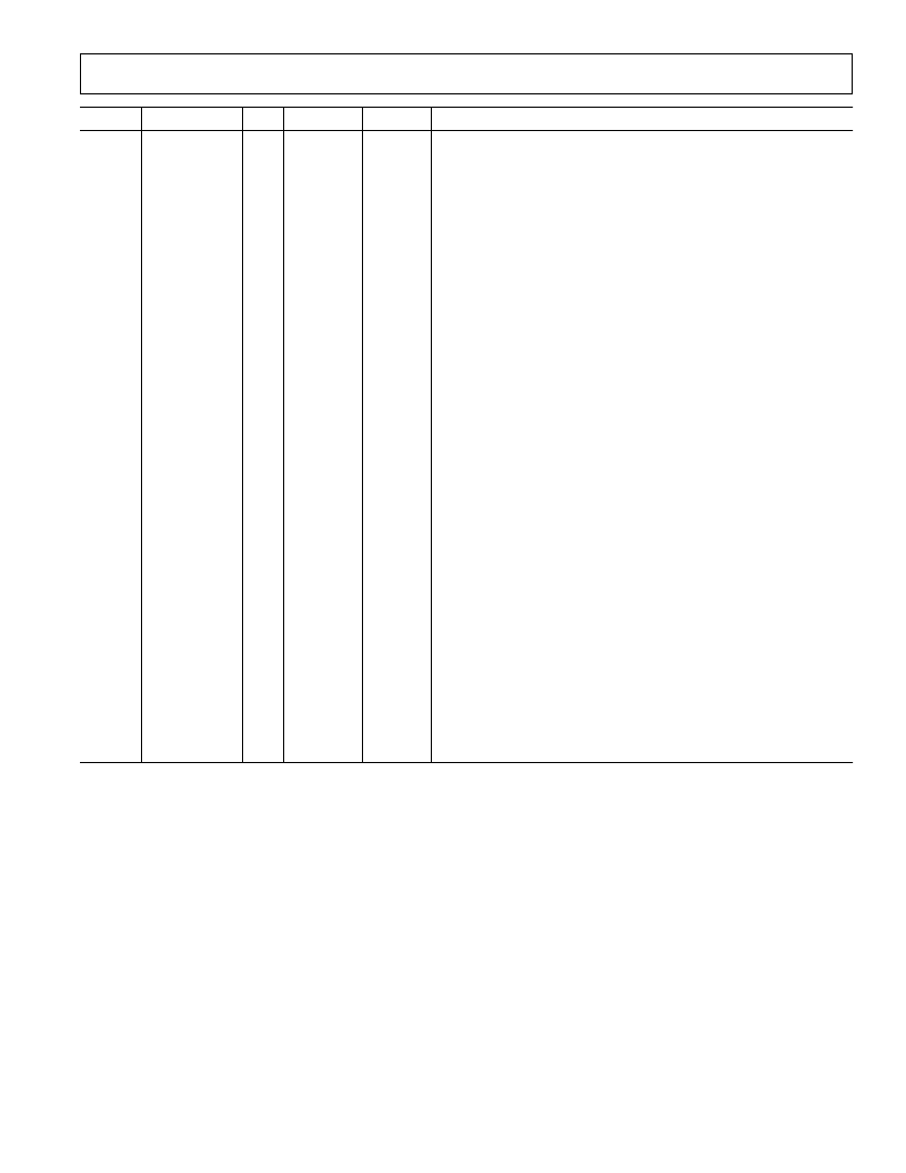
Address
Name
R/W
# of Bits
Default
Description
0Eh
ZXTOUT
R/W
12
FFFh
Zero Cross Timeout. If no zero crossings are detected on Channel 2
within a time period specified by this 12-bit register, the interrupt
request line (
IRQ
) will be activated. The maximum timeout period is
0.15 second—see Zero Crossing Detection section.
Sag Line Cycle register. This 8-bit register specifies the number of
consecutive half-line cycles the signal on Channel 2 must be below
SAGLVL before the
SAG
output is activated—see Voltage Sag Detec-
tion section.
Interrupt Enable register. ADE7759 interrupts may be deactivated at
any time by setting the corresponding bit in this 8-bit Enable register
to Logic 0. The Status register will continue to register an interrupt
event even if disabled. However, the
IRQ
output will not be
activated—see Interrupts section.
Sag Voltage Level. An 8-bit write to this register determines at what
peak signal level on Channel 2 the
SAG
pin will become active. The
signal must remain low for the number of cycles specified in the
SAGCYC register before the
SAG
pin is activated—see Line Voltage
Sag Detection section.
Temperature register. This is an 8-bit register which contains the result of
the latest temperature conversion—see Temperature Measurement section.
Line Cycle Energy Accumulation Mode Half-Cycle register. This 14-
bit register is used during line cycle energy accumulation mode to set
the number of half-line cycles active energy is accumulated—see Line
Cycle Energy Accumulation Mode section.
Line Cycle Energy Accumulation Mode Active Energy register. This
40-bit register accumulates active energy during line cycle energy
accumulation mode. The number of half-line cycles is set by the
LINECYC register—see Line Cycle Energy Accumulation Mode section.
CF Frequency Divider Numerator register. The output frequency on
the CF pin is adjusted by writing to this 12-bit read/write register—see
Energy to Frequency Conversion section
.
Checksum register. This 6-bit read-only register is equal to the sum of
all the ones in the previous read—see Serial Read Operation section
.
Die Revision register. This 8-bit read-only register contains the revision
number of the silicon.
0Fh
SAGCYC
R/W
8
FFh
10h
IRQEN
R/W
8
40h
11h
SAGLVL
R/W
8
0h
12h
TEMP
R
8
0h
13h
LINECYC
R/W
14
3FFFh
14h
LENERGY
R
40
0h
15h
CFNUM
R/W
12
0h
1Eh
CHKSUM
R
6
0h
1Fh
DIEREV
R
8
01h
REGISTER DESCRIPTIONS
All ADE7759 functionality is accessed via the on-chip registers. Each register is accessed by first writing to the Communications
register and then transferring the register data. A full description of the serial interface protocol is given in the Serial Interface section
of this data sheet.
Communications Register
The Communications register is an 8-bit, write-only register that controls the serial data transfer between the ADE7759 and the host
processor. All data transfer operations must begin with a write to the Communications register. The data written to the Communica-
tions register determines whether the next operation is a read or a write and which register is being accessed. Table V outlines the bit
designations for the Communications register.
相關(guān)PDF資料 |
PDF描述 |
|---|---|
| ADE7760ARSRL | Energy Metering IC with On-Chip Fault Detection |
| ADE7760 | 8-Channel 14-Bit Single-Supply Voltage-Output DAC; Package: LQFP (10x10mm); No of Pins: 52; Temperature Range: Industrial |
| ADE7760ARS | Energy Metering IC with On-Chip Fault Detection |
| ADE7762 | Polyphase Energy Metering IC with Phase Drop Indication |
| ADE7762ARW | Polyphase Energy Metering IC with Phase Drop Indication |
相關(guān)代理商/技術(shù)參數(shù) |
參數(shù)描述 |
|---|---|
| ADE7759ARS | 功能描述:IC ENERGY METERING 1PHASE 20SSOP RoHS:否 類(lèi)別:集成電路 (IC) >> PMIC - 能量測(cè)量 系列:- 產(chǎn)品培訓(xùn)模塊:Lead (SnPb) Finish for COTS Obsolescence Mitigation Program 標(biāo)準(zhǔn)包裝:2,500 系列:* |
| ADE7759ARSRL | 功能描述:IC ENERGY METERING 1PHASE 20SSOP RoHS:否 類(lèi)別:集成電路 (IC) >> PMIC - 能量測(cè)量 系列:- 產(chǎn)品培訓(xùn)模塊:Lead (SnPb) Finish for COTS Obsolescence Mitigation Program 標(biāo)準(zhǔn)包裝:2,500 系列:* |
| ADE7759ARSZ | 功能描述:IC ENERGY METERING 1PHASE 20SSOP RoHS:是 類(lèi)別:集成電路 (IC) >> PMIC - 能量測(cè)量 系列:- 產(chǎn)品培訓(xùn)模塊:Lead (SnPb) Finish for COTS Obsolescence Mitigation Program 標(biāo)準(zhǔn)包裝:2,500 系列:* |
| ADE7759ARSZRL | 功能描述:IC ENERGY METERING 1PHASE 20SSOP RoHS:是 類(lèi)別:集成電路 (IC) >> PMIC - 能量測(cè)量 系列:- 產(chǎn)品培訓(xùn)模塊:Lead (SnPb) Finish for COTS Obsolescence Mitigation Program 標(biāo)準(zhǔn)包裝:2,500 系列:* |
| ADE7760 | 制造商:AD 制造商全稱(chēng):Analog Devices 功能描述:Energy Metering IC with On-Chip Fault Detection |
發(fā)布緊急采購(gòu),3分鐘左右您將得到回復(fù)。