- 您現(xiàn)在的位置:買賣IC網(wǎng) > PDF目錄373980 > ADE7759 (Analog Devices, Inc.) Active Energy Metering IC with di/dt Sensor Interface PDF資料下載
參數(shù)資料
| 型號(hào): | ADE7759 |
| 廠商: | Analog Devices, Inc. |
| 英文描述: | Active Energy Metering IC with di/dt Sensor Interface |
| 中文描述: | 有源電能計(jì)量IC的di / dt傳感器接口 |
| 文件頁數(shù): | 12/32頁 |
| 文件大小: | 530K |
| 代理商: | ADE7759 |
第1頁第2頁第3頁第4頁第5頁第6頁第7頁第8頁第9頁第10頁第11頁當(dāng)前第12頁第13頁第14頁第15頁第16頁第17頁第18頁第19頁第20頁第21頁第22頁第23頁第24頁第25頁第26頁第27頁第28頁第29頁第30頁第31頁第32頁
REV. 0
ADE7759
–12–
It is also possible to adjust offset errors on Channel 1 and Channel 2
by writing to the Offset Correction registers (CH1OS and CH2OS
respectively). These registers allow channel offsets in the range
±
24 mV to
±
50 mV (depending on the gain setting) to be removed.
Note that it is not necessary to perform an offset correction in an
energy measurement application if HPF1 Channel 1 is switched
on. Figure 6 shows the effect of offsets on the real power calcula-
tion. As seen in Figure 6, an offset on Channel 1 and Channel 2
will contribute a dc component after multiplication. Since this
dc component is extracted by LPF2 to generate the Active (Real)
Power information, the offsets will have contributed an error to
the Active Power calculation. This problem is easily avoided by
enabling HPF1 in Channel 1. By removing the offset from at
least one channel, no error component is generated at dc by the
multiplication. Error terms at cos(
ω
t) are removed by LPF2 and
by integration of the Active Power signal in the Active Energy
register (AENERGY[39:0])—see Energy Calculation section.
DC COMPONENT (INCLUDING ERROR TERM)
IS EXTRACTED BY THE LPF FOR REAL
POWER CALCULATION
I
OS
V
V
OS
I
V
OS
I
OS
V I
2
0
2
Figure 6. Effect of Channel Offsets on the Real
Power Calculation
The contents of the Offset Correction registers are 6-bit, sign,
and magnitude coded. The weighting of the LSB size depends
on the gain setting, i.e., 1, 2, 4, 8, or 16. Table II shows the
correctable offset span for each of the gain settings and the LSB
weight (mV) for the Offset Correction registers. The maximum
value that can be written to the offset correction registers is
±
31
decimal—see Figure 7.
Table II. Offset Correction Range
Gain
Correctable Span
±
50 mV
±
37 mV
±
30 mV
±
26 mV
±
24 mV
LSB Size
1
2
4
8
16
1.61 mV/LSB
1.19 mV/LSB
0.97 mV/LSB
0.84 mV/LSB
0.77 mV/LSB
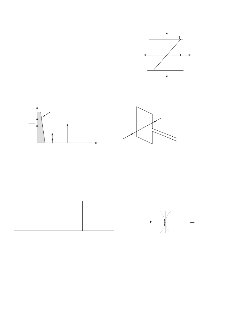
Figure 7 shows the relationship between the Offset Correction
register contents and the offset (mV) on the analog inputs for a
gain setting of one. In order to perform an offset adjustment, the
analog inputs should be first connected to AGND, and there
should be no signal on either Channel 1 or Channel 2. A read
from Channel 1 or Channel 2 using the Waveform register will
give an indication of the offset in the channel. This offset can be
canceled by writing an equal but opposite offset value to the
relevant offset register. The offset correction can be confirmed by
performing another read. Note that when adjusting the offset of
Channel 1, the digital integrator and the HPF1 should be disabled.
CH1OS[5:0]
SIGN + 5 BITS
+50mV
OFFSET
ADJUST
3Fh
00h
1Fh
–
50mV
0mV
SIGN + 5 BITS
01,1111b
11,1111b
Figure 7. Channel Offset Correction Range (Gain = 1)
di/dt CURRENT SENSOR AND DIGITAL INTEGRATOR
di/dt sensor detects changes in magnetic field caused by ac
current. Figure 8 shows the principle of a di/dt current sensor.
MAGNETIC FIELD CREATED BY CURRENT
(DIRECTLY PROPORTIONAL TO CURRENT)
EMF (ELECTROMOTIVE FORCE)
INDUCED BY CHANGES IN
MAGNETIC FLUX DENSITY (di/dt)
+
–
Figure 8. Principle of a di/dt Current Sensor
The flux density of a magnetic field induced by a current is directly
proportional to the magnitude of the current. The changes in
the magnetic flux density passing through a conductor loop
generate an electromotive force (EMF) between the two ends of
the loop. The EMF is a voltage signal that is proportional to the
di/dt of the current. The voltage output from the di/dt current
sensor is determined by the mutual inductance between the
current-carrying conductor and the di/dt sensor. Figure 9 shows
the mutual inductance produces a di/dt signal at the output of
the sensor.
+
MUTUAL INDUCTANCE M
i(t)
–
v = M
di(t)
dt
Figure 9. Mutual Inductance Between the di/dt
Sensor and the Current Carrying Conductor
The current signal needs to be recovered from the di/dt signal
before it can be used for active power calculation. An integrator
is therefore necessary to restore the signal to its original form.
The ADE7759 has a built-in digital integrator to recover the
current signal from the di/dt sensor. The digital integrator on
Channel 1 is switched on by default when the ADE7759 is
powered up. Setting the MSB of the CH1OS register to 0 will
turn off the integrator. Figures 10 to 13 show the magnitude and
phase response of the digital integrator.
相關(guān)PDF資料 |
PDF描述 |
|---|---|
| ADE7760ARSRL | Energy Metering IC with On-Chip Fault Detection |
| ADE7760 | 8-Channel 14-Bit Single-Supply Voltage-Output DAC; Package: LQFP (10x10mm); No of Pins: 52; Temperature Range: Industrial |
| ADE7760ARS | Energy Metering IC with On-Chip Fault Detection |
| ADE7762 | Polyphase Energy Metering IC with Phase Drop Indication |
| ADE7762ARW | Polyphase Energy Metering IC with Phase Drop Indication |
相關(guān)代理商/技術(shù)參數(shù) |
參數(shù)描述 |
|---|---|
| ADE7759ARS | 功能描述:IC ENERGY METERING 1PHASE 20SSOP RoHS:否 類別:集成電路 (IC) >> PMIC - 能量測(cè)量 系列:- 產(chǎn)品培訓(xùn)模塊:Lead (SnPb) Finish for COTS Obsolescence Mitigation Program 標(biāo)準(zhǔn)包裝:2,500 系列:* |
| ADE7759ARSRL | 功能描述:IC ENERGY METERING 1PHASE 20SSOP RoHS:否 類別:集成電路 (IC) >> PMIC - 能量測(cè)量 系列:- 產(chǎn)品培訓(xùn)模塊:Lead (SnPb) Finish for COTS Obsolescence Mitigation Program 標(biāo)準(zhǔn)包裝:2,500 系列:* |
| ADE7759ARSZ | 功能描述:IC ENERGY METERING 1PHASE 20SSOP RoHS:是 類別:集成電路 (IC) >> PMIC - 能量測(cè)量 系列:- 產(chǎn)品培訓(xùn)模塊:Lead (SnPb) Finish for COTS Obsolescence Mitigation Program 標(biāo)準(zhǔn)包裝:2,500 系列:* |
| ADE7759ARSZRL | 功能描述:IC ENERGY METERING 1PHASE 20SSOP RoHS:是 類別:集成電路 (IC) >> PMIC - 能量測(cè)量 系列:- 產(chǎn)品培訓(xùn)模塊:Lead (SnPb) Finish for COTS Obsolescence Mitigation Program 標(biāo)準(zhǔn)包裝:2,500 系列:* |
| ADE7760 | 制造商:AD 制造商全稱:Analog Devices 功能描述:Energy Metering IC with On-Chip Fault Detection |
發(fā)布緊急采購,3分鐘左右您將得到回復(fù)。