- 您現(xiàn)在的位置:買賣IC網(wǎng) > PDF目錄373980 > ADE7754ARRL (ANALOG DEVICES INC) ADE7754 PDF資料下載
參數(shù)資料
| 型號: | ADE7754ARRL |
| 廠商: | ANALOG DEVICES INC |
| 元件分類: | 模擬信號調(diào)理 |
| 英文描述: | ADE7754 |
| 中文描述: | SPECIALTY ANALOG CIRCUIT, PDSO24 |
| 封裝: | MS-013AD, SOIC-24 |
| 文件頁數(shù): | 19/44頁 |
| 文件大小: | 630K |
| 代理商: | ADE7754ARRL |
第1頁第2頁第3頁第4頁第5頁第6頁第7頁第8頁第9頁第10頁第11頁第12頁第13頁第14頁第15頁第16頁第17頁第18頁當(dāng)前第19頁第20頁第21頁第22頁第23頁第24頁第25頁第26頁第27頁第28頁第29頁第30頁第31頁第32頁第33頁第34頁第35頁第36頁第37頁第38頁第39頁第40頁第41頁第42頁第43頁第44頁
REV. PrG 01/03
PRELIMINARY TECHNICAL DATA
ADE7754
–
19
–
ACTIVE POWER CALCULATION
Electrical power is defined as the rate of energy flow from
source to load. It is given by the product of the voltage and
current waveforms. The resulting waveform is called the
instantaneous power signal and it is equal to the rate of energy
flow at every instant of time. The unit of power is the watt or
joules/sec. Equation 5 gives an expression for the instanta-
neous power signal in an ac system.
ω
v(t)
t
= 2V sin(
)
(3)
i(t)
where V = rms voltage, I = rms current.
t
= 2I sin(
)
ω
(4)
p
(t)
p
(t)
v(t)
i(t)
=
= VI - VI cos(
×
2 t
)
(5)
The average power over an integral number of line cycles (n)
is given by the expression in Equation 6.
P =
1
nT
p(t)dt=VI
0
nT
∫
(6)
where T is the line cycle period.
P is referred to as the Active or Real Power. Note that the
active power is equal to the DC component of the instanta-
neous power signal
p(t)
in Equation 5
, i.e., VI. This is the
relationship used to calculate active power in the ADE7754
for each phase. The instantaneous power signal
p(t)
is
generated by multiplying the current and voltage signals in
each phase. The DC component of the instantaneous power
signal in each phase (A, B and C) is then extracted by LPF2
(Low Pass Filter) to obtain the active power information on
each phase. This process is illustrated graphically on Figure
20. In a polyphase system, the total electrical power is simply
the sum of the real power in all active phases. The different
solutions available to process the total active power are
discussed in the following paragraph.
Voltage
2
=
Current
i(t)
=
Instantaneous
Power Signal
Active Real Power
Signal = V x I
V. I.
00000h
1A36E2Eh
D1B717h
)
sin(
2
t
I
ω
)
sin(
t
V
v(t)
ω
)
2
cos(
t
I
V
I
V
p(t)
ω
×
×
=
Figure 20– Active Power Calculation
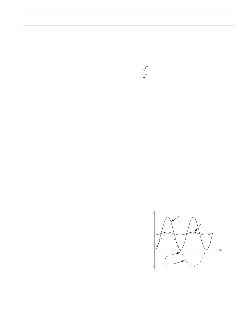
Voltage RMS Gain Adjust
The Voltage Gain register (AVGAIN[11:0], BVGAIN and
CVGAIN) have an effect on the Apparent Power and voltage
rms values. It is not recommended to calibrate the voltage
rms measurements with these registers. The conversion of
the voltage rms registers values to Volts has to be done in an
external Micro-controller with a specific Volt/LSB constant
for each phase -
see Calibration of a 3-phase meter based on the
ADE7754
. Due to gain mismatches between phases, the
calibration of the Volt/LSB constant has to be done for each
phase separately. One point calibration is sufficient for this
calibration. The Voltage Gain registers are aimed to ease the
calibration of the apparent energy calculation in MODE 1
and 2 of the VAMODE register.
If the VGAIN registers are used for Apparent Power calibra-
tion (VAMOD bits in VAMode register = 1 or 2), the voltage
rms values are changed by Voltage Gain register value as
described in the expression below:
Voltage RMS
gister Phase A
RMS
AVGAIN
2
12
Re
=
×
+
1
For example, when 7FFh is written to the Voltage Gain
register, the ADC output is scaled up by +50%. 7FFh =
2047d, 2047/2
12
= 0.5. Similarly, 800h = -2047 Dec (signed
2’s Complement) and ADC output is scaled by –50%. These
two examples are illustrated graphically in Figure 19.
Voltage RMS offset compensation
The ADE7754 incorporates a voltage RMS offset compen-
sation for each phase (AVRMSOS, BVRMSOS and
CVRMSOS). These are 12-bit 2-complement signed regis-
ters which can be used to remove offsets in the voltage RMS
calculations. An offset may exist in the RMS calculation due
to input noises and offsets in the input samples. The offset
calibration allows the contents of the VRMS registers to be
maintained at zero when no voltage is applied.
n LSB of the Voltage RMS offset are equivalent to 64 x n LSB
of the voltage RMS register. Assuming that the maximum
value from the Voltage RMS calculation is 1,898,124d with
full scale AC inputs, then 1 LSB of the voltage RMS offset
represents 0.07% of measurement error at -26dB down of full
scale.
V
V
VRMSOS
rms
rms
=
+
×
0
64
where V
rmso
is the RMS measurement without offset correc-
tion.
The voltage rms offset compensation should be done by
testing the rms results at two non-zero input levels. One
measurement can be done close to full scale and the other at
approximately Full scale/10. The voltage offset compensa-
tion can then be derived from these measurements -
see
Calibration of a 3-phase meter based on the ADE7754
.
相關(guān)PDF資料 |
PDF描述 |
|---|---|
| ADE7755AN-REF | Energy Metering IC with Pulse Output |
| ADE7755ARSRL | Energy Metering IC with Pulse Output |
| ADE7755 | Energy Metering IC with Pulse Output |
| ADE7755ARS | Energy Metering IC with Pulse Output |
| ADE7756EB | Evaluation Board Documentation AD7756 Energy metering IC |
相關(guān)代理商/技術(shù)參數(shù) |
參數(shù)描述 |
|---|---|
| ADE7754ARZ | 功能描述:IC ENERGY METERING 3PHASE 24SOIC RoHS:是 類別:集成電路 (IC) >> PMIC - 能量測量 系列:- 產(chǎn)品培訓(xùn)模塊:Lead (SnPb) Finish for COTS Obsolescence Mitigation Program 標準包裝:2,500 系列:* |
| ADE7754ARZRL | 功能描述:IC ENERGY METERING 3PHASE 24SOIC RoHS:是 類別:集成電路 (IC) >> PMIC - 能量測量 系列:- 產(chǎn)品培訓(xùn)模塊:Lead (SnPb) Finish for COTS Obsolescence Mitigation Program 標準包裝:2,500 系列:* |
| ADE7755 | 制造商:AD 制造商全稱:Analog Devices 功能描述:Energy Metering IC with Pulse Output |
| ADE7755AARSRL | 制造商:Analog Devices 功能描述:ENERGY METERING IC WITH P - Tape and Reel |
| ADE7755AN | 制造商:Rochester Electronics LLC 功能描述: 制造商:Analog Devices 功能描述: |
發(fā)布緊急采購,3分鐘左右您將得到回復(fù)。