- 您現(xiàn)在的位置:買賣IC網(wǎng) > PDF目錄1894 > AD9859YSVZ-REEL7 (Analog Devices Inc)IC DDS DAC 10BIT 400MSPS 48TQFP PDF資料下載
參數(shù)資料
| 型號: | AD9859YSVZ-REEL7 |
| 廠商: | Analog Devices Inc |
| 文件頁數(shù): | 22/24頁 |
| 文件大小: | 0K |
| 描述: | IC DDS DAC 10BIT 400MSPS 48TQFP |
| 產(chǎn)品培訓模塊: | Direct Digital Synthesis Tutorial Series (1 of 7): Introduction Direct Digital Synthesizer Tutorial Series (7 of 7): DDS in Action Direct Digital Synthesis Tutorial Series (3 of 7): Angle to Amplitude Converter Direct Digital Synthesis Tutorial Series (6 of 7): SINC Envelope Correction Direct Digital Synthesis Tutorial Series (4 of 7): Digital-to-Analog Converter Direct Digital Synthesis Tutorial Series (2 of 7): The Accumulator |
| 標準包裝: | 500 |
| 分辨率(位): | 10 b |
| 主 fclk: | 400MHz |
| 調(diào)節(jié)字寬(位): | 32 b |
| 電源電壓: | 1.71 V ~ 1.96 V |
| 工作溫度: | -40°C ~ 105°C |
| 安裝類型: | 表面貼裝 |
| 封裝/外殼: | 48-TQFP 裸露焊盤 |
| 供應(yīng)商設(shè)備封裝: | 48-TQFP 裸露焊盤(7x7) |
| 包裝: | 帶卷 (TR) |

AD9859
Rev. A | Page 7 of 24
PIN FUNCTION DESCRIPTIONS
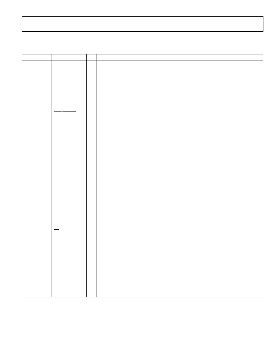
Table 3. Pin Function Descriptions—48-Lead TQFP/EP
Pin No.
Mnemonic
I/O
Description
1
I/O UPDATE
I
The rising edge transfers the contents of the internal buffer memory to the I/O registers. This
pin must be set up and held around the SYNC_CLK output signal.
2, 34
DVDD
I
Digital Power Supply Pins (1.8 V).
3, 33, 42, 47,
48
DGND
I
Digital Power Ground Pins.
4, 6, 13, 16, 18,
19, 25, 27, 29
AVDD
I
Analog Power Supply Pins (1.8 V).
5, 7, 14, 15, 17,
22, 26, 28, 30,
31, 32
AGND
I
Analog Power Ground Pins.
8
OSC/
I
REFCLK
Complementary Reference Clock/Oscillator Input. When the REFCLK port is operated in single-
ended mode, REFCLKB should be decoupled to AVDD with a 0.1 F capacitor.
9
OSC/REFCLK
I
Reference Clock/Oscillator Input. See the Clock Input section for details on the
OSCILLATOR/REFCLK operation.
10
CRYSTAL OUT
O
Output of the Oscillator Section.
11
CLKMODESELECT
I
Control Pin for the Oscillator Section. When high, the oscillator section is enabled. When low,
the oscillator section is bypassed.
12
LOOP_FILTER
I
This pin provides the connection for the external zero compensation network of the REFCLK
multiplier’s PLL loop filter. The network consists of a 1 k resistor in series with a 0.1 F
capacitor tied to AVDD.
20
IOUT
O
Complementary DAC Output. Should be biased through a resistor to AVDD, not AGND.
21
IOUT
O
DAC Output. Should be biased through a resistor to AVDD, not AGND.
23
DACBP
I
DAC Band Gap Decoupling Pin. A 0.1 μF capacitor to AGND is recommended.
24
DAC_R
SET
I
A resistor (3.92 k nominal) connected from AGND to DAC_R
SET establishes the reference
current for the DAC.
35
PWRDWNCTL
I
Input Pin Used as an External Power-Down Control (see Table 8 for details).
36
RESET
I
Active High Hardware Reset Pin. Asserting the RESET pin forces the AD9859 to the initial state,
as described in the I/O port register map.
37
IOSYNC
I
Asynchronous Active High Reset of the Serial Port Controller. When high, the current I/O
operation is immediately terminated, enabling a new I/O operation to commence once IOSYNC
is returned low. If unused, ground this pin; do not allow this pin to float.
38
SDO
O
When operating the I/O port as a 3-wire serial port, this pin serves as the serial data output.
When operated as a 2-wire serial port, this pin is unused and can be left unconnected.
39
CS
I
This pin functions as an active low chip select that allows multiple devices to share the I/O bus.
40
SCLK
I
This pin functions as the serial data clock for I/O operations.
41
SDIO
I/O
When operating the I/O port as a 3-wire serial port, this pin serves as the serial data input only.
When operated as a 2-wire serial port, this pin is the bidirectional serial data pin.
43
DVDD_I/O
I
Digital Power Supply (for I/O Cells Only, 3.3 V).
44
SYNC_IN
I
Input Signal Used to Synchronize Multiple AD9859s. This input is connected to the SYNC_CLK
output of a master AD9859.
45
SYNC_CLK
O
Clock Output Pin Serves as a Synchronizer for External Hardware.
46
OSK
I
Input Pin Used to Control the Direction of the Shaped On-Off Keying Function when
Programmed for Operation. OSK is synchronous to the SYNC_CLK pin. When OSK is not
programmed, this pin should be tied to DGND.
<49>
AGND
I
The exposed paddle on the bottom of the package is a ground connection for the DAC and
must be attached to AGND in any board layout.
相關(guān)PDF資料 |
PDF描述 |
|---|---|
| AD9880KSTZ-100 | IC INTERFACE/HDMI 100MHZ 100LQFP |
| AD9882KSTZ-140 | IC INTERFACE/DVI 100MHZ 100LQFP |
| AD9883ABSTZ-RL140 | IC INTERFACE FLAT 140MHZ 80LQFP |
| AD9887AKSZ-100 | IC INTRFACE ANALOG/DVI 160-MQFP |
| AD9887AKSZ-140 | IC INTRFACE ANALOG/DVI 160-MQFP |
相關(guān)代理商/技術(shù)參數(shù) |
參數(shù)描述 |
|---|---|
| AD9859YSVZ-REEL71 | 制造商:AD 制造商全稱:Analog Devices 功能描述:400 MSPS, 10-Bit, 1.8 V CMOS Direct Digital Synthesizer |
| AD9860 | 制造商:AD 制造商全稱:Analog Devices 功能描述:Mixed-Signal Front-End (MxFE⑩) Processor for Broadband Communications |
| AD9860BST | 制造商:Analog Devices 功能描述:Mixed Signal Front End 128-Pin LQFP 制造商:Rochester Electronics LLC 功能描述:10B MIXED SIGNAL FRONT END MXFE PROCESSO - Tape and Reel |
| AD9860BSTRL | 制造商:Analog Devices 功能描述:Mixed Signal Front End 128-Pin LQFP T/R 制造商:Rochester Electronics LLC 功能描述:10B MIXED SIGNAL FRONT END MXFE PROCESSO - Tape and Reel |
| AD9860BSTZ | 功能描述:IC PROCESSOR FRONT END 128LQFP RoHS:是 類別:RF/IF 和 RFID >> RF 前端 (LNA + PA) 系列:- 產(chǎn)品培訓模塊:Lead (SnPb) Finish for COTS Obsolescence Mitigation Program 標準包裝:250 系列:- RF 型:GPS 頻率:1575.42MHz 特點:- 封裝/外殼:48-TQFP 裸露焊盤 供應(yīng)商設(shè)備封裝:48-TQFP 裸露焊盤(7x7) 包裝:托盤 |
發(fā)布緊急采購,3分鐘左右您將得到回復。