- 您現(xiàn)在的位置:買賣IC網(wǎng) > PDF目錄375248 > AD9661AKR-REEL (ANALOG DEVICES INC) Laser Diode Driver with Light Power Control PDF資料下載
參數(shù)資料
| 型號: | AD9661AKR-REEL |
| 廠商: | ANALOG DEVICES INC |
| 元件分類: | 其它接口 |
| 英文描述: | Laser Diode Driver with Light Power Control |
| 中文描述: | SPECIALTY INTERFACE CIRCUIT, PDSO28 |
| 封裝: | PLASTIC, SOIC-28 |
| 文件頁數(shù): | 2/12頁 |
| 文件大小: | 174K |
| 代理商: | AD9661AKR-REEL |
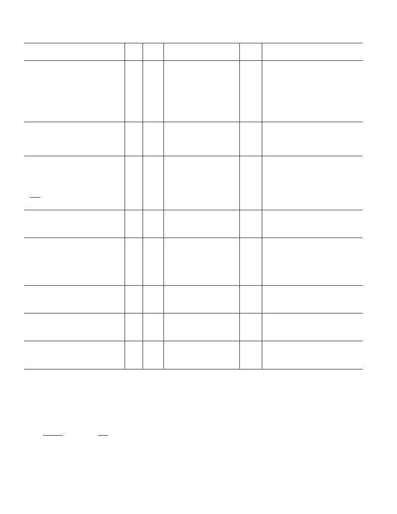
AD9661A–SPECIFICATIONS
T est
Level
AD9661AKR
T yp
Parameter
T emp
Min
Max
Units
Conditions
ANALOG INPUT
Input Voltage Range, POWER LEVEL
Input Bias Current, POWER LEVEL
Analog Bandwidth, Control Loop
1
Input Voltage Range, LEVEL SHIFT IN
Input Bias Current, LEVEL SHIFT IN
Analog Bandwidth, Level Shift
2
Level Shift Offset
Level Shift Gain
OUT PUT S
Output Current, I
OUT
Output Compliance Range
Idle Current
Disable Current
SWIT CHING PERFORMANCE
Maximum Pulse Rate
Output Propagation Delay (t
PD
), Rising
3
Output Propagation Delay (t
PD
), Falling
3
Output Current Rise T ime
4
Output Current Fall T ime
5
CAL
Aperture Delay
6
Disable T ime
7
HOLD NODE
Input Bias Current
Input Voltage Range
Minimum External Hold Cap
T T L /CMOS INPUT S
8
Logic “1” Voltage
Logic “1” Voltage
Logic “0” Voltage
Logic “0” Voltage
Logic “1” Current
Logic “0” Current
BANDGAP REFERENCE
Output Voltage (V
REF
)
T emperature Coefficient
Output Current
SENSE IN
Current Gain
Voltage
Input Resistance
POWER SUPPLY
+V
S
Voltage
+V
S
Current
IV
I
V
IV
I
V
I
I
Full
+25
°
C
+25
°
C
Full
+25
°
C
Full
+25
°
C
+25
°
C
V
REF
–50
V
REF
+ 1.6
+50
V
μ
A
MHz
V
μ
A
MHz
mV
V/V
25
C
HOLD
= 33 pF, R
F
= 1 k
, C
F
= 2 pF
0.1
–10
1.6
0
130
–32
0.95
+32
1.05
1.0
I
IV
I
IV
+25
°
C
+25
°
C
+25
°
C
+25
°
C
120
2.50
mA
V
mA
μ
A
V
OUT
= 2.5 V
5.25
5.0
1.0
2
PULSE = LOW, DISABLE = LOW
PULSE = LOW, DISABLE = HIGH
V
IV
IV
IV
IV
IV
IV
+25
°
C
Full
Full
Full
Full
Full
+25
°
C
200
3.9
3.7
1.5
1.5
13
3
MHz
ns
ns
ns
ns
ns
ns
Output Current –3 dB
2.9
3.2
5.0
4.3
2.0
2.0
5
I
IV
V
+25
°
C
Full
Full
–200
V
REF
200
V
REF
+ 1.6
nA
V
pF
V
HOLD
= 2.5 V
Open-Loop Application Only
25
I
IV
I
IV
I
I
+25
°
C
Full
+25
°
C
Full
+25
°
C
+25
°
C
2.0
2.0
V
V
V
V
μ
A
mA
0.8
0.8
10
–10
–1.5
V
HIGH
= 5.0 V
V
LOW
= 0.8 V
I
V
V
+25
°
C
+25
°
C
+25
°
C
1.6
1.8
–0.1
1.9
V
mV/
°
C
mA
–0.5
1.0
I
I
V
+25
°
C
+25
°
C
+25
°
C
0.95
0.7
1
1.0
<150
1.02
1.3
mA/mA
V
I
I
+25
°
C
+25
°
C
4.75
60
5.00
75
5.25
95
V
mA
DISABLE = HIGH, V
HOLD
= V
REF
,
V
S
= 5.0 V
NOT ES
1
Based on rise time of closed-loop pulse response. See Performance Curves.
2
Based on rise time of pulse response.
3
Propagation delay measured from the 50% of the rising/falling transition of WRIT E PULSE to the 50% point of the rising/falling edge of the output modulation
current.
4
Rise time measured between the 10% and 90% points of the rising transition of the modulation current.
5
Fall time measured between the 10% and 90% points of the falling transition of the modulation current.
6
Aperture Delay is measured from the 50% point of the rising edge of WRIT E PULSE to the time when the output modulation begins to recalibrate, WRIT E CAL is
held during this test.
7
Disable T ime is measured from the 50% point of the rising edge of DISABLE to the 50% point of the falling transition of the output current. Fall time during disable
is similar to fall time during normal operation.
8
PULSE,
PULSE2
, DISABLE, and
CAL
are T T L/CMOS compatible inputs.
Specifications subject to change without notice.
REV. 0
–2–
(+V
S
= +5 V, Temperature = +25
8
C unless otherwse noted)
相關(guān)PDF資料 |
PDF描述 |
|---|---|
| AD9661AKR | Laser Diode Driver with Light Power Control |
| AD9662 | 3-Channel Laser Diode Driver with Oscillator |
| AD9701 | 250 MSPS Video Digital-to-Analog Converter(250MSPS視頻D/A轉(zhuǎn)換器) |
| AD9748 | Analog Devices: Data Converters: DAC 8-Bit, 10 ns to 100 ns Converters Selection Table |
| AD9748XCP | 8-Bit, 165 MSPS TxDAC D/A Converter |
相關(guān)代理商/技術(shù)參數(shù) |
參數(shù)描述 |
|---|---|
| AD9662 | 制造商:Analog Devices 功能描述:- Bulk |
| AD9662ARQZ | 制造商:Analog Devices 功能描述:LASER DRVR 3-CH 16QSOP - Rail/Tube |
| AD9662ARQZ-REEL7 | 功能描述:IC LASER DIODE DRIVER 3CH 16QSOP RoHS:是 類別:集成電路 (IC) >> PMIC - 激光驅(qū)動器 系列:- 產(chǎn)品培訓(xùn)模塊:Lead (SnPb) Finish for COTS Obsolescence Mitigation Program 標(biāo)準(zhǔn)包裝:60 系列:- 類型:激光二極管驅(qū)動器 數(shù)據(jù)速率:- 通道數(shù):4 電源電壓:3.3V 電流 - 電源:- 電流 - 調(diào)制:- 電流 - 偏置:- 工作溫度:0°C ~ 70°C 封裝/外殼:40-TQFN 裸露焊盤 供應(yīng)商設(shè)備封裝:40-TQFN EP 包裝:托盤 安裝類型:表面貼裝 |
| AD9664 | 制造商:AD 制造商全稱:Analog Devices 功能描述:4-Channel LVDS Dual-Output Laser Diode Driver with Oscillator |
| AD9664ACPDNZ-REEL | 制造商:Analog Devices 功能描述:LASER DRVR 4-CH 32LFCSP EP - Tape and Reel |
發(fā)布緊急采購,3分鐘左右您將得到回復(fù)。