- 您現(xiàn)在的位置:買賣IC網(wǎng) > PDF目錄16993 > AD9481-PCBZ (Analog Devices Inc)BOARD EVAL 8BIT 250MSPS 44-TQFP PDF資料下載
參數(shù)資料
| 型號(hào): | AD9481-PCBZ |
| 廠商: | Analog Devices Inc |
| 文件頁數(shù): | 23/28頁 |
| 文件大?。?/td> | 0K |
| 描述: | BOARD EVAL 8BIT 250MSPS 44-TQFP |
| 標(biāo)準(zhǔn)包裝: | 1 |
| ADC 的數(shù)量: | 1 |
| 位數(shù): | 8 |
| 采樣率(每秒): | 250M |
| 數(shù)據(jù)接口: | 并聯(lián) |
| 輸入范圍: | 1 Vpp |
| 在以下條件下的電源(標(biāo)準(zhǔn)): | 439mW @ 250MSPS |
| 工作溫度: | -40°C ~ 85°C |
| 已用 IC / 零件: | AD9481 |
| 已供物品: | 板 |
| 相關(guān)產(chǎn)品: | AD9481BSUZ-250-ND - IC ADC 8BIT 250MSPS 3.3V 44-TQFP |
第1頁第2頁第3頁第4頁第5頁第6頁第7頁第8頁第9頁第10頁第11頁第12頁第13頁第14頁第15頁第16頁第17頁第18頁第19頁第20頁第21頁第22頁當(dāng)前第23頁第24頁第25頁第26頁第27頁第28頁
AD9481
Rev. 0 | Page 4 of 28
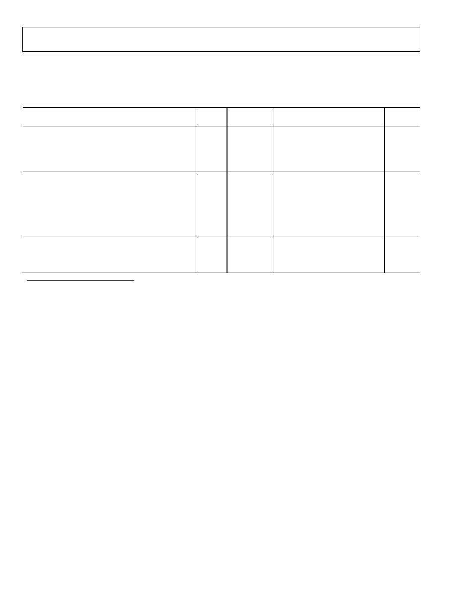
DIGITAL SPECIFICATIONS
AVDD = 3.3 V, DRVDD = 3.3 V; TMIN = 40°C, TMAX = +85°C, AIN = 1 dBFS, full scale = 1.0 V, internal reference, differential analog and
clock inputs, unless otherwise noted.
Table 2.
AD9481-250
Parameter
Temp
Test Level
Min
Typ
Max
Unit
CLOCK AND DS INPUTS (CLK+, CLK, DS+, DS)
Differential Input
Full
IV
200
mV p-p
Common-Mode Voltage1
Full
VI
1.38
1.5
1.68
V
Input Resistance
Full
VI
4.2
5.5
6.0
k
Input Capacitance
25°C
V
4
pF
LOGIC INPUTS (PDWN, S1)
Logic 1 Voltage
Full
IV
2.0
V
Logic 0 Voltage
Full
IV
0.8
V
Logic 1 Input Current
Full
VI
±160
A
Logic 0 input Current
Full
VI
10
A
Input Resistance
25°C
V
30
k
Input Capacitance
25°C
V
4
pF
DIGITAL OUTPUTS
Logic 1 Voltage2
Full
VI
DRVDD 0.05
mV
Logic 0 Voltage
Full
VI
0.05
V
Output Coding
Full
IV
Twos complement or binary
1 The common mode for CLOCK inputs can be externally set, such that 0.9 V < CLK ± < 2.6 V.
2 Capacitive loading only.
相關(guān)PDF資料 |
PDF描述 |
|---|---|
| VI-J44-EY | CONVERTER MOD DC/DC 48V 50W |
| CDB5525 | EVAL BOARD FOR CS5525 |
| 222A111-25/86-0 | BOOT MOLDED |
| VI-J0Z-EY | CONVERTER MOD DC/DC 2V 20W |
| CDB5526 | EVAL BOARD FOR CS5526 |
相關(guān)代理商/技術(shù)參數(shù) |
參數(shù)描述 |
|---|---|
| AD9483 | 制造商:AD 制造商全稱:Analog Devices 功能描述:Triple 8-Bit, 140 MSPS A/D Converter |
| AD9483/PCB | 制造商:Analog Devices 功能描述: |
| AD9483KS-100 | 制造商:Analog Devices 功能描述:ADC Triple Flash 100Msps 8-bit Parallel 100-Pin MQFP 制造商:Analog Devices 功能描述:ADC TRIPLE FLASH 100MSPS 8BIT PARALLEL 100MQFP - Trays |
| AD9483KS-140 | 制造商:Analog Devices 功能描述:Triple ADC Flash 140Msps 8-bit Parallel 100-Pin MQFP 制造商:Analog Devices 功能描述:ADC TRIPLE FLASH 140MSPS 8BIT PARALLEL 100MQFP - Trays |
| AD9484 | 制造商:AD 制造商全稱:Analog Devices 功能描述:8-Bit, 500 MSPS, 1.8 V Analog-to-Digital Converter Excellent linearity |
發(fā)布緊急采購,3分鐘左右您將得到回復(fù)。