- 您現(xiàn)在的位置:買賣IC網(wǎng) > PDF目錄375241 > AD802 (Analog Devices, Inc.) Clock Recovery and Data Retiming Phase-Locked Loop(時(shí)鐘恢復(fù)和重定時(shí)PLL) PDF資料下載
參數(shù)資料
| 型號(hào): | AD802 |
| 廠商: | Analog Devices, Inc. |
| 英文描述: | Clock Recovery and Data Retiming Phase-Locked Loop(時(shí)鐘恢復(fù)和重定時(shí)PLL) |
| 中文描述: | 時(shí)鐘恢復(fù)和數(shù)據(jù)重定時(shí)鎖相環(huán)(時(shí)鐘恢復(fù)和重定時(shí)鎖相環(huán)) |
| 文件頁(yè)數(shù): | 4/12頁(yè) |
| 文件大小: | 258K |
| 代理商: | AD802 |
AD800/AD802
REV. B
–4–
T he PLL must provide a clock signal which tracks this phase
modulation in order to accurately retime jittered data. In order
for the VCO output to have a phase modulation which tracks
the input jitter, some modulation signal must be generated at
the output of the phase detector (see Figure 21). T he
modulation output from the phase detector can only be
produced by a phase error between the data input and the clock
input. Hence, the PLL can never perfectly track jittered data.
However, the magnitude of the phase error depends on the gain
around the loop. At low frequencies the integrator provides very
high gain, and thus very large jitter can be tracked with small
phase errors between input data and recovered clock. At
frequencies closer to the loop bandwidth, the gain of the
integrator is much smaller, and thus less input jitter can be
tolerated. T he PLL data output will have a bit error rate less
than 1
3
10
–10
when in lock and retiming input data that has the
specified jitter applied to it.
Jitter T ransfer
T he PLL exhibits a low-pass filter response to jitter applied to
its input data.
Bandwidth
T his describes the frequency at which the PLL attenuates
sinusoidal input jitter by 3 dB.
Peaking
T his describes the maximum jitter gain of the PLL in dB.
Damping Factor,
z
ζ
describes how the PLL will track an input signal with a phase
step. A greater value of
ζ
corresponds to less overshoot in the
PLL response to a phase step.
ζ
is a standard constant in second
order feedback systems.
Acquisition T ime
T his is the transient time, measured in bit periods, required for
the PLL to lock on input data from its free-running state.
Symmetry
Symmetry is calculated as (100
3
on time)/period, where on
time equals the time that the clock signal is greater than the
midpoint between its “0” level and its “1” level.
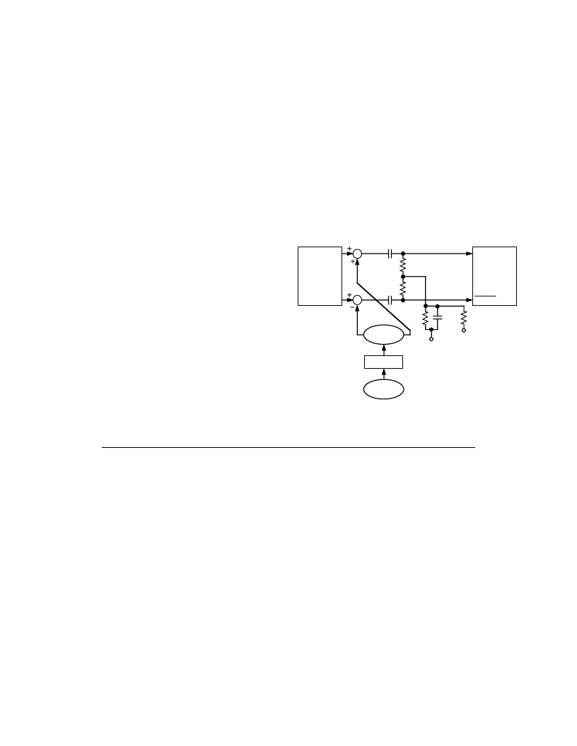
Bit E rror Rate vs. Signal-to-Noise Ratio
T he AD800 and AD802 were designed to operate with standard
ECL signal levels at the data input. Although not recom-
mended, smaller input signals are tolerable. Figure 8, 14, and
20 show the bit error rate performance versus input signal-to-
noise ratio for input signal amplitudes of full 900 mV ECL, and
decreased amplitudes of 80 mV and 20 mV. Wideband ampli-
tude noise is summed with the data signals as shown in Figure
2. T he full ECL and 80 mV signals give virtually indistinguish-
able results. T he 20 mV signals also provide adequate perfor-
mance when in lock, but signal acquisition may be impaired.
∑
POWER
COMBINER
∑
0.47
μ
F
50
50
0.47
μ
F
POWER
COMBINER
75
1.0
μ
F
180
POWER
SPLITTER
FILTER
NOISE
SOURCE
100MHz – AD802-155
33MHz – AD800-52
GND
–5.2V
D.U.T.
AD800/AD802
DATA IN
DATA IN
DIFFERENTIAL
SIGNAL
SOURCE
Figure 2. Bit Error Rate vs. Signal-to-Noise Ratio Test:
Block Diagram
USING T HE AD800 AND T HE AD802 SE RIE S
Ground Planes
Use of one ground plane for connections to both analog and
digital grounds is recommended. Output signal sensitivity to
power supply noise (PECL configuration, Figure 22) is less
using one ground plane than when using separate analog and
digital ground planes.
Power Supply Connections
Use of a 10
μ
F tantalum capacitor between V
EE
and ground is
recommended.
Use of 0.1
μ
F ceramic capacitors between IC power supply or
substrate pins and ground is recommended. Power supply
decoupling should take place as close to the IC as possible.
Refer to schematics, Figure 22 and Figure 26, for advised
connections.
Sensitivity of IC output signals (PECL configuration,
Figure 22) to high frequency power supply noise (at 2
3
the
nominal data rate) can be reduced through the connection of
signals AV
CC
and V
CC1
, and the addition of a bypass network.
T he type of bypass network to consider depends on the noise
tolerance required. T he more complex bypass network schemes
tolerate greater power supply noise levels. Refer to Figures 23
and 24 for bypassing schemes and power supply sensitivity
curves.
T ransmission Lines
Use of 50
transmission lines are recommended for DAT AIN,
CLK OUT , DAT AOUT , and FRAC signals.
T erminations
T ermination resistors should be used for DAT AIN, CLK OUT ,
DAT AOUT , and FRAC signals. Metal, thick film, 1% tolerance
resistors are recommended. T ermination resistors for the
DAT AIN signals should be placed as close as possible to the
DAT AIN pins.
Connections from V
EE
to lead resistors for DAT AIN, DAT A-
OUT , FRAC, and CLK OUT signals should be individual, not
daisy chained. T his will avoid crosstalk on these signals.
Loop Damping Capacitor, C
D
A ceramic capacitor may be used for the loop damping
capacitor.
Input Buffer
Use of an input buffer, such as a 10H116 Line Receiver IC, is
suggested for an application where the DAT AIN signals do not
come directly from an ECL gate, or where noise immunity on
the DAT AIN signals is an issue.
相關(guān)PDF資料 |
PDF描述 |
|---|---|
| AD8013 | Single Supply Low Power,Triple Video Amplifier(單電源,低功耗,三通道視頻放大器) |
| AD8014 | 400 MHz Low Power High Performance Amplifier |
| AD8021ARMZ | Low Noise, High Speed Amplifier for 16-Bit Systems |
| AD8021ARMZ-REEL | Low Noise, High Speed Amplifier for 16-Bit Systems |
| AD8021ARMZ-REEL7 | Low Noise, High Speed Amplifier for 16-Bit Systems |
相關(guān)代理商/技術(shù)參數(shù) |
參數(shù)描述 |
|---|---|
| AD80201Z | 制造商:Analog Devices 功能描述: |
| AD80206ABCPZ-125 | 制造商:Analog Devices 功能描述:ANAAD80206ABCPZ-125 14BIT IF DIVERSITY R |
| AD8021 | 制造商:AD 制造商全稱:Analog Devices 功能描述:Dual 8-,10-,12-Bit High Bandwidth Multiplying DACs with Serial Interface |
| AD8021_06 | 制造商:AD 制造商全稱:Analog Devices 功能描述:Low Noise, High Speed Amplifier for 16-Bit Systems |
發(fā)布緊急采購(gòu),3分鐘左右您將得到回復(fù)。