- 您現(xiàn)在的位置:買(mǎi)賣(mài)IC網(wǎng) > PDF目錄373922 > AD7873BCP (ANALOG DEVICES INC) Touch Screen Digitizer PDF資料下載
參數(shù)資料
| 型號(hào): | AD7873BCP |
| 廠商: | ANALOG DEVICES INC |
| 元件分類(lèi): | 消費(fèi)家電 |
| 英文描述: | Touch Screen Digitizer |
| 中文描述: | SPECIALTY CONSUMER CIRCUIT, QCC16 |
| 封裝: | 4 X 4 MM, MO-220VGGC, LFCSP-16 |
| 文件頁(yè)數(shù): | 14/28頁(yè) |
| 文件大?。?/td> | 657K |
| 代理商: | AD7873BCP |
第1頁(yè)第2頁(yè)第3頁(yè)第4頁(yè)第5頁(yè)第6頁(yè)第7頁(yè)第8頁(yè)第9頁(yè)第10頁(yè)第11頁(yè)第12頁(yè)第13頁(yè)當(dāng)前第14頁(yè)第15頁(yè)第16頁(yè)第17頁(yè)第18頁(yè)第19頁(yè)第20頁(yè)第21頁(yè)第22頁(yè)第23頁(yè)第24頁(yè)第25頁(yè)第26頁(yè)第27頁(yè)第28頁(yè)
AD7873
ANALOG INPUT
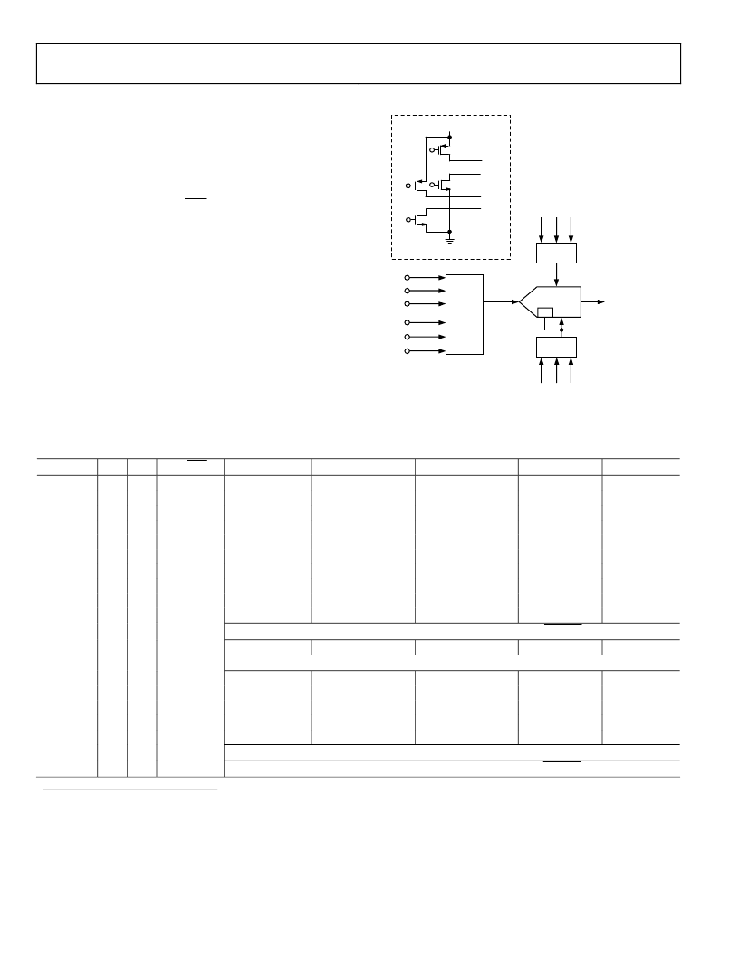
Figure 26 shows an equivalent circuit of the analog input
structure of the AD7873, which contains a block diagram of the
input multiplexer, the differential input of the ADC, and the
differential reference.
Rev. D | Page 14 of 28
Table 5 shows the multiplexer address corresponding to each
analog input, both for the SER/DFR bit in the control register
set high and low. The control bits are provided serially to the
device via the DIN pin. For more information on the control
register, see the Control Register section.
When the converter enters hold mode, the voltage difference
between the +IN and –IN inputs (see Figure 26) is captured on
the internal capacitor array. The input current on the analog
inputs depends on the conversion rate of the device. During the
sample period, the source must charge the internal sampling
capacitor (typically 37 pF). Once the capacitor is fully charged,
there is no further input current. The rate of charge transfer
from the analog source to the converter is a function of
conversion rate.
0
X+ Y+
REF
INT/
EXT
X– Y– GND
6-TO-1
MUX
3-TO-1
MUX
3-TO-1
MUX
IN+
IN+
IN– REF–
REF+
ADC CORE
DATA OUT
V
CC
Y–
Y+
X+
X–
ON-CHIP SWITCHES
X+
Y+
Y–
V
BAT
AUX
TEMP
Figure 26. Equivalent Analog Input Circuit
Table 5. Analog Input, Reference, and Touch Screen Control
A2
A1
A0
SER/ DFR
0
0
0
1
0
0
1
1
0
1
0
1
0
1
1
1
1
0
0
1
1
0
1
1
1
1
0
1
1
1
1
1
0
0
0
0
0
0
1
0
0
1
0
0
0
1
1
0
1
0
0
0
1
0
1
0
1
1
0
0
1
1
1
0
Analog Input
TEMP0
X+
VBAT
X+ (Z1)
Y– (Z2)
Y+
AUX
TEMP1
Invalid Address. Test Mode: Switches out the Temp0 diode to the PENIRQ pin.
X+
OFF
Invalid Address
X+ (Z1)
X+ OFF
X– ON
Y– (Z2)
X+ OFF
X– ON
Y+
ON
Outputs Identity Code, 1000 0000 0000.
Invalid address. Test mode: Switches out the Temp1 diode to the PENIRQ pin.
X Switches
OFF
OFF
OFF
X+ OFF
X– ON
X+ OFF
X– ON
ON
OFF
OFF
Y Switches
OFF
ON
OFF
Y+ ON
Y– OFF
Y+ ON
Y– OFF
OFF
OFF
OFF
+REF
1
V
REF
V
REF
V
REF
V
REF
V
REF
V
REF
V
REF
V
REF
–REF
1
GND
GND
GND
GND
GND
GND
GND
GND
ON
Y+
Y–
Y+ ON
Y– OFF
Y+ ON
Y– OFF
OFF
Y+
Y+
X+
X–
X–
X–
1
Internal node, not directly accessible by the user.
相關(guān)PDF資料 |
PDF描述 |
|---|---|
| AD7873BRQ | Touch Screen Digitizer |
| AD7874 | 4-Channel, 12-Bit Simultaneous Sampling Data Acquisition System(LC2MOS 4通道,12位同時(shí)采樣DAS) |
| AD7878SQ | IC 1:10 CLOCK DRIVER 20-QSOP |
| AD7878 | LC2MOS Complete 12-Bit 100 kHz Sampling ADC with DSP Interface |
| AD7878AQ | LC2MOS Complete 12-Bit 100 kHz Sampling ADC with DSP Interface |
相關(guān)代理商/技術(shù)參數(shù) |
參數(shù)描述 |
|---|---|
| AD7873BCP-REEL | 制造商:Analog Devices 功能描述:TOUCH SCREEN DIGITIZER |
| AD7873BCP-REEL7 | 制造商:Analog Devices 功能描述:TOUCH SCREEN DIGITIZER 制造商:Analog Devices 功能描述:2.7V 12-BIT TOUCH SCREEN DIGITIZER I.C. - Tape and Reel |
| AD7873BCPZ | 制造商:Analog Devices 功能描述:TOUCH SCREEN DIGITIZER |
| AD7873BRQ | 制造商:Analog Devices 功能描述:TOUCH SCREEN DIGITIZER |
| AD7873BRQ-REEL | 制造商:Analog Devices 功能描述:TOUCH SCREEN DIGITIZER |
發(fā)布緊急采購(gòu),3分鐘左右您將得到回復(fù)。