- 您現(xiàn)在的位置:買賣IC網(wǎng) > PDF目錄375235 > AD6459 (Analog Devices, Inc.) GSM 3 V Receiver IF Subsystem PDF資料下載
參數(shù)資料
| 型號(hào): | AD6459 |
| 廠商: | Analog Devices, Inc. |
| 英文描述: | GSM 3 V Receiver IF Subsystem |
| 中文描述: | 3伏的GSM接收機(jī)中頻子系統(tǒng) |
| 文件頁(yè)數(shù): | 12/12頁(yè) |
| 文件大?。?/td> | 314K |
| 代理商: | AD6459 |
AD6459
–12–
REV. 0
C
P
AD6459 EVALUATION BOARD
The AD6459 evaluation board (Figure 27) consists of a
AD6459, ground plane, I/O connectors, and a 19.5 MHz band
pass filter. The RF, LO and FREF ports are terminated in 50
to provide a broadband match or external signal generators.
The board provides SMA connectors for the RF, LO, demodu-
lator reference, mixer output and IF input signals. The MXOP
and IFIP connectors are left unconnected and are provided as a
testing convenience. Footprints for broadband matching trans-
formers and matching components are also provided to aid in
stage breakout testing.
The remaining low frequency signals, including the I and Q
interface, bias and power connections are made via a dual row
pin header that acts as an Interface Connector located along the
edges of the board. An on-board gain-reference 1.2 V biasing
option is provided via a single jumper, J1. The evaluation board
will not function without this jumper unless an external bias
GREF is provided from an external reference that is normally
provided by the associated ADC.
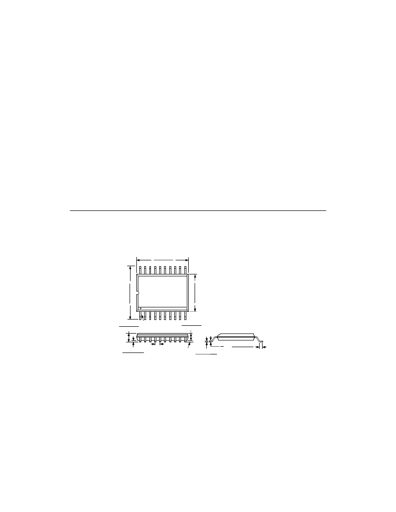
OUTLINE DIMENSIONS
Dimensions shown in inches and (mm).
20
11
10
1
0.295 (7.50)
0.271 (6.90)
0
0
0
0
PIN 1
SEATING
PLANE
0.008 (0.203)
0.002 (0.050)
0.07 (1.78)
0.066 (1.67)
0.0256
(0.65)
BSC
0.078 (1.98)
0.068 (1.73)
0.009 (0.229)
0.005 (0.127)
0.037 (0.94)
0.022 (0.559)
8
°
0
°
Full Path Configuration
As received, the board is configured for full-path evaluation
from RFHI to the I and Q outputs. The one-pole LC resonant
circuit provided represents a simple, yet balanced, IF bandpass
filtering approach. The filter supplied is centered at 19.5 MHz,
a common GSM intermediate frequency. Table I highlights the
filter component values for other IF frequencies. RFHI and
RFLO are true differential inputs, however for testing conve-
nience, the RFLO terminal of the AD6459 is ac referenced to
ground on the evaluation board. The GAIN bias input, which is
bypassed with a 10 nF capacitor, is brought out to the interface
connector. The PRUP input is provided with a 20 k
pull up
resistor to V
POS
that activates the board.
The four differential I and Q outputs are brought out uncondi-
tioned, directly to the interface connector. A high impedance,
high bandwidth FET-type probe should be used when measur-
ing the I and Q ports. Excessive capacitive or resistive loading of
these ports will severely limit the video bandwidth and signal
swing. The demodulator PLL filter installed on the evaluation
board (R8, C10) can accommodate the full VFQO lock range
specified.
相關(guān)PDF資料 |
PDF描述 |
|---|---|
| AD6459ARS | GSM 3 V Receiver IF Subsystem |
| AD6630 | Differential, Low Noise IF Gain Block with Output Clamping(差分,低噪聲中頻增益塊) |
| AD6650 | Diversity IF to Baseband GSM/EDGE Narrowband Receiver |
| AD6650PCB | Diversity IF to Baseband GSM/EDGE Narrowband Receiver |
| AD6650BBC1 | Diversity IF to Baseband GSM/EDGE Narrowband Receiver |
相關(guān)代理商/技術(shù)參數(shù) |
參數(shù)描述 |
|---|---|
| AD6459ARS | 制造商:Analog Devices 功能描述:RF Receiver N-QAM/N-PSK/TDMA 3.3V/5V 20-Pin SSOP |
| AD6459ARS-REEL | 制造商:Analog Devices 功能描述:RF Receiver N-QAM/N-PSK/TDMA 3.3V/5V 20-Pin SSOP T/R |
| AD645A | 制造商:AD 制造商全稱:Analog Devices 功能描述:Low Noise, Low Drift FET Op Amp |
| AD645AH | 制造商:AD 制造商全稱:Analog Devices 功能描述:Low Noise, Low Drift FET Op Amp |
| AD645B | 制造商:AD 制造商全稱:Analog Devices 功能描述:Low Noise, Low Drift FET Op Amp |
發(fā)布緊急采購(gòu),3分鐘左右您將得到回復(fù)。