- 您現(xiàn)在的位置:買賣IC網(wǎng) > PDF目錄4489 > A3PE600-1PQG208 (Microsemi SoC)IC FPGA 600000 GATES 208-PQFP PDF資料下載
參數(shù)資料
| 型號(hào): | A3PE600-1PQG208 |
| 廠商: | Microsemi SoC |
| 文件頁數(shù): | 92/162頁 |
| 文件大?。?/td> | 0K |
| 描述: | IC FPGA 600000 GATES 208-PQFP |
| 標(biāo)準(zhǔn)包裝: | 24 |
| 系列: | ProASIC3E |
| RAM 位總計(jì): | 110592 |
| 輸入/輸出數(shù): | 147 |
| 門數(shù): | 600000 |
| 電源電壓: | 1.425 V ~ 1.575 V |
| 安裝類型: | 表面貼裝 |
| 工作溫度: | 0°C ~ 70°C |
| 封裝/外殼: | 208-BFQFP |
| 供應(yīng)商設(shè)備封裝: | 208-PQFP(28x28) |
第1頁第2頁第3頁第4頁第5頁第6頁第7頁第8頁第9頁第10頁第11頁第12頁第13頁第14頁第15頁第16頁第17頁第18頁第19頁第20頁第21頁第22頁第23頁第24頁第25頁第26頁第27頁第28頁第29頁第30頁第31頁第32頁第33頁第34頁第35頁第36頁第37頁第38頁第39頁第40頁第41頁第42頁第43頁第44頁第45頁第46頁第47頁第48頁第49頁第50頁第51頁第52頁第53頁第54頁第55頁第56頁第57頁第58頁第59頁第60頁第61頁第62頁第63頁第64頁第65頁第66頁第67頁第68頁第69頁第70頁第71頁第72頁第73頁第74頁第75頁第76頁第77頁第78頁第79頁第80頁第81頁第82頁第83頁第84頁第85頁第86頁第87頁第88頁第89頁第90頁第91頁當(dāng)前第92頁第93頁第94頁第95頁第96頁第97頁第98頁第99頁第100頁第101頁第102頁第103頁第104頁第105頁第106頁第107頁第108頁第109頁第110頁第111頁第112頁第113頁第114頁第115頁第116頁第117頁第118頁第119頁第120頁第121頁第122頁第123頁第124頁第125頁第126頁第127頁第128頁第129頁第130頁第131頁第132頁第133頁第134頁第135頁第136頁第137頁第138頁第139頁第140頁第141頁第142頁第143頁第144頁第145頁第146頁第147頁第148頁第149頁第150頁第151頁第152頁第153頁第154頁第155頁第156頁第157頁第158頁第159頁第160頁第161頁第162頁
ProASIC3E Flash Family FPGAs
Revision 13
2-21
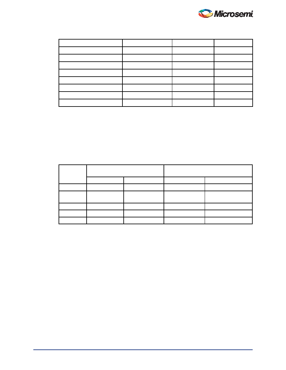
3.3 V GTL+
35 mA
12
–
2.5 V GTL+
33 mA
15
–
HSTL (I)
8 mA
50
HSTL (II)
15 mA 4
25
SSTL2 (I)
15 mA
27
31
SSTL2 (II)
18 mA
13
15
SSTL3 (I)
14 mA
44
69
SSTL3 (II)
21 mA
18
32
Table 2-20 I/O Weak Pull-Up/Pull-Down Resistances
Minimum and Maximum Weak Pull-Up/Pull-Down Resistance Values
VCCI
R((WEAK PULL-UP)1
(
)
R(WEAK PULL-DOWN)2
(
)
Min.
Max.
Min.
Max.
3.3 V
10 k
45 k
10 k
45 k
3.3 V (Wide
Range I/Os)
10 k
45 k
10 k
45 k
2.5 V
11 k
55 k
12 k
74 k
1.8 V
18 k
70 k
17 k
110 k
1.5 V
19 k
90 k
19 k
140 k
Notes:
1. R(WEAK PULL-UP-MAX) = (VCCImax – VOHspec) / I(WEAK PULL-UP-MIN)
2. R(WEAK PULL-DOWN-MAX) = (VOLspec) / I(WEAK PULL-DOWN-MIN)
Table 2-19 I/O Output Buffer Maximum Resistances1 (continued)
Standard
Drive Strength
RPULL-DOWN ()2
RPULL-UP ()3
Notes:
1. These maximum values are provided for informational reasons only. Minimum output buffer resistance
values depend on VCCI, drive strength selection, temperature, and process. For board design
considerations and detailed output buffer resistances, use the corresponding IBIS models located on the
Microsemi SoC Products Group website at www.microsemi.com/soc/techdocs/models/ibis.html.
2. R(PULL-DOWN-MAX) = (VOLspec) / IOLspec
3. R(PULL-UP-MAX) = (VCCImax – VOHspec) / IOHspec
4. Output drive strength is below JEDEC specification.
相關(guān)PDF資料 |
PDF描述 |
|---|---|
| A3PE600-1PQ208 | IC FPGA 600000 GATES 208-PQFP |
| EP4CE30F23I7N | IC CYCLONE IV FPGA 30K 484FBGA |
| EP4CE30F23C6N | IC CYCLONE IV FPGA 30K 484FBGA |
| GCB70DHBR | CONN EDGECARD 140PS R/A .050 SLD |
| ACM40DRMI-S288 | CONN EDGECARD EXTEND 80POS 0.156 |
相關(guān)代理商/技術(shù)參數(shù) |
參數(shù)描述 |
|---|---|
| A3PE600-1PQG208I | 功能描述:IC FPGA 600000 GATES 208-PQFP RoHS:是 類別:集成電路 (IC) >> 嵌入式 - FPGA(現(xiàn)場(chǎng)可編程門陣列) 系列:ProASIC3E 標(biāo)準(zhǔn)包裝:40 系列:SX-A LAB/CLB數(shù):6036 邏輯元件/單元數(shù):- RAM 位總計(jì):- 輸入/輸出數(shù):360 門數(shù):108000 電源電壓:2.25 V ~ 5.25 V 安裝類型:表面貼裝 工作溫度:0°C ~ 70°C 封裝/外殼:484-BGA 供應(yīng)商設(shè)備封裝:484-FPBGA(27X27) |
| A3PE600-1PQG896 | 制造商:ACTEL 制造商全稱:Actel Corporation 功能描述:ProASIC3E Flash Family FPGAs |
| A3PE600-1PQG896ES | 制造商:ACTEL 制造商全稱:Actel Corporation 功能描述:ProASIC3E Flash Family FPGAs |
| A3PE600-1PQG896I | 制造商:ACTEL 制造商全稱:Actel Corporation 功能描述:ProASIC3E Flash Family FPGAs |
| A3PE600-1PQG896PP | 制造商:ACTEL 制造商全稱:Actel Corporation 功能描述:ProASIC3E Flash Family FPGAs |
發(fā)布緊急采購,3分鐘左右您將得到回復(fù)。