- 您現(xiàn)在的位置:買賣IC網(wǎng) > PDF目錄25526 > 95V2F857AKLFT (INTEGRATED DEVICE TECHNOLOGY INC) 95V SERIES, PLL BASED CLOCK DRIVER, 10 TRUE OUTPUT(S), 0 INVERTED OUTPUT(S), QCC40 PDF資料下載
參數(shù)資料
| 型號(hào): | 95V2F857AKLFT |
| 廠商: | INTEGRATED DEVICE TECHNOLOGY INC |
| 元件分類: | 時(shí)鐘及定時(shí) |
| 英文描述: | 95V SERIES, PLL BASED CLOCK DRIVER, 10 TRUE OUTPUT(S), 0 INVERTED OUTPUT(S), QCC40 |
| 封裝: | LEAD FREE, MLF-40 |
| 文件頁(yè)數(shù): | 7/13頁(yè) |
| 文件大?。?/td> | 146K |
| 代理商: | 95V2F857AKLFT |
第1頁(yè)第2頁(yè)第3頁(yè)第4頁(yè)第5頁(yè)第6頁(yè)當(dāng)前第7頁(yè)第8頁(yè)第9頁(yè)第10頁(yè)第11頁(yè)第12頁(yè)第13頁(yè)
3
ICS95V2F857A
1065A—02/03/05
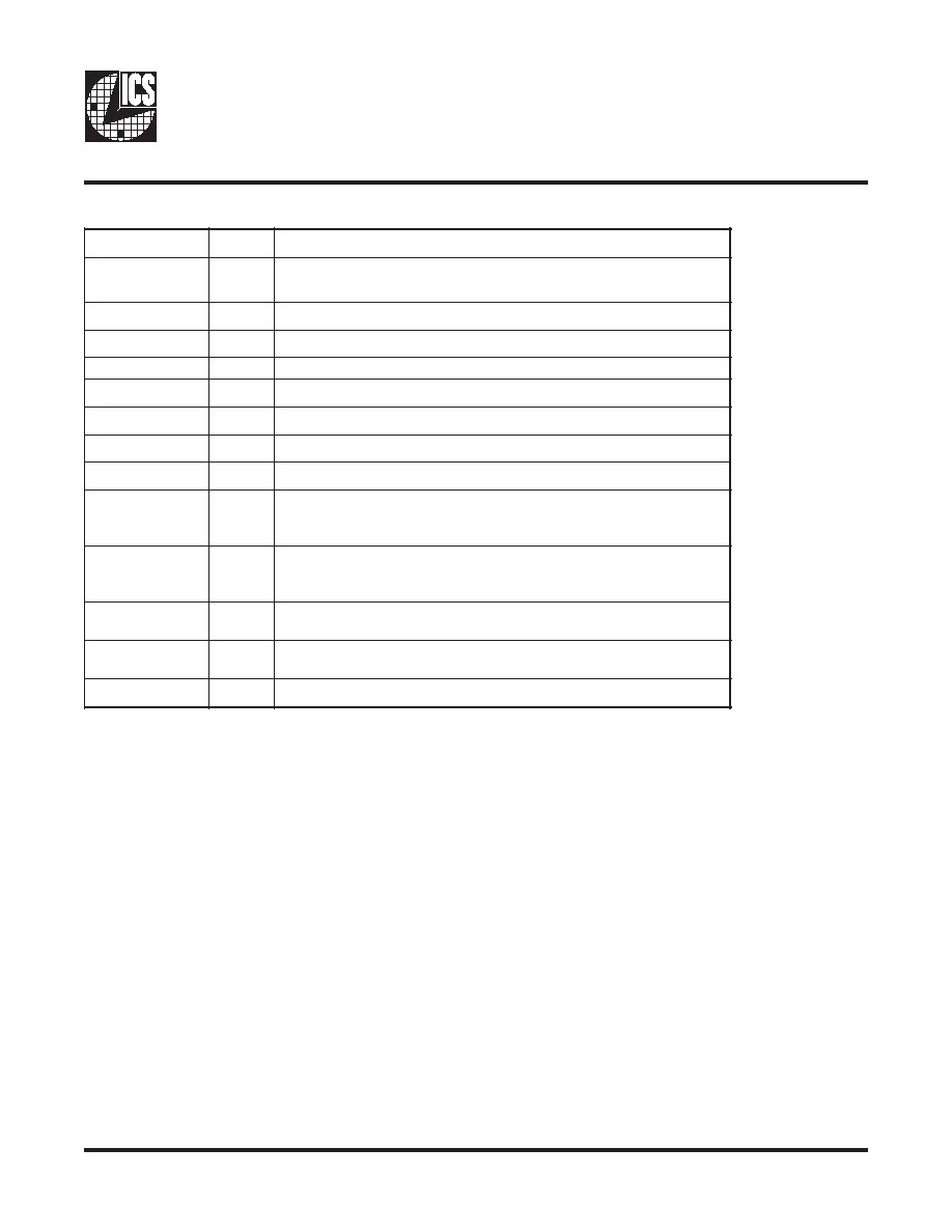
Pin Descriptions
E
M
A
N
I
PE
P
Y
TN
O
I
T
P
I
R
C
S
E
D
D
VR
W
PV
5
.
2
,
y
l
p
u
s
r
e
w
o
P
D
N
GR
W
Pd
n
u
o
r
G
D
V
AR
W
PV
5
.
2
,
y
l
p
u
s
r
e
w
o
p
g
o
l
a
n
A
D
N
G
AR
W
Pd
n
u
o
r
g
o
l
a
n
A
)
0
:
9
(
T
K
L
CT
U
Os
t
u
p
t
u
o
r
i
a
p
l
a
i
t
n
e
r
e
f
i
d
f
o
k
c
o
l
C
"
e
u
r
T
"
)
0
:
9
(
C
K
L
CT
U
Os
t
u
p
t
u
o
r
i
a
p
l
a
i
t
n
e
r
e
f
i
d
f
o
s
k
c
o
l
c
"
y
r
a
t
n
e
m
e
l
p
m
o
C
"
C
N
I
_
K
L
CN
It
u
p
n
i
k
c
o
l
c
e
c
n
e
r
e
f
e
r
"
y
r
a
t
n
e
m
e
l
p
m
o
C
"
T
N
I
_
K
L
CN
It
u
p
n
i
k
c
o
l
c
e
c
n
e
r
e
f
e
r
"
e
u
r
T
"
C
T
U
O
_
B
FT
U
O
t
I
.
k
c
a
b
d
e
f
l
a
n
r
e
t
x
e
r
o
f
d
e
t
a
c
i
d
e
d
,
t
u
p
t
u
o
k
c
a
b
d
e
F
"
y
r
a
t
n
e
m
e
l
p
m
o
C
"
d
e
r
i
w
e
b
t
s
u
m
t
u
p
t
u
o
s
i
h
T
.
K
L
C
e
h
t
s
a
y
c
n
e
u
q
e
r
f
e
m
a
s
e
h
t
a
s
e
h
c
t
i
w
s
C
N
I
_
B
F
o
t
T
U
O
_
B
FT
U
O
s
e
h
c
t
i
w
s
t
I
.
k
c
a
b
d
e
f
l
a
n
r
e
t
x
e
r
o
f
d
e
t
a
c
i
d
e
d
,
t
u
p
t
u
o
k
c
a
b
d
e
F
"
e
u
r
T
"
o
t
d
e
r
i
w
e
b
t
s
u
m
t
u
p
t
u
o
s
i
h
T
.
K
L
C
e
h
t
s
a
y
c
n
e
u
q
e
r
f
e
m
a
s
e
h
t
a
T
N
I
_
B
F
T
N
I
_
B
FN
I
r
o
f
L
P
l
a
n
r
e
t
n
i
e
h
t
o
t
l
a
n
g
i
s
k
c
a
b
d
e
f
s
e
d
i
v
o
r
p
,
t
u
p
n
i
k
c
a
b
d
e
F
"
e
u
r
T
"
r
o
r
e
s
a
h
p
e
t
a
n
i
m
il
e
o
t
T
N
I
_
K
L
C
h
t
i
w
n
o
i
t
a
z
i
n
o
r
h
c
n
y
s
C
N
I
_
B
FN
I
L
P
l
a
n
r
e
t
n
i
e
h
t
o
t
l
a
n
g
i
s
e
d
i
v
o
r
p
,
t
u
p
n
i
k
c
a
b
d
e
F
"
y
r
a
t
n
e
m
e
l
p
m
o
C
"
r
o
r
e
s
a
h
p
e
t
a
n
i
m
il
e
o
t
C
N
I
_
K
L
C
h
t
i
w
n
o
i
t
a
z
i
n
o
r
h
c
n
y
s
r
o
f
#
D
PN
It
u
p
n
i
S
O
M
C
V
L
.
n
w
o
D
r
e
w
o
P
This PLL Clock Buffer is designed for a VDD of 2.5V, an AVDD of 2.5V and differential data input and output levels.
The ICS95V2F857A is a zero delay buffer that distributes a differential clock input pair (CLK_INC, CLK_INT) to ten
differential pair of clock outputs (CLKT[0:9], CLKC[0:9]) and one differential pair feedback clock output (FB_OUT,
FB_OUTC).The clock outputs are controlled by the input clocks (CLK_INC, CLK_INT), the feedback clocks (FB_INT,
FB_INC), the 2.5-V LVCMOS input (PD#) and the Analog Power input (AVDD).When input (PD#) is low while power is
applied, the receivers are disabled, the PLL is turned off and the differential clock outputs are tri-stated. When AVDD
is grounded, the PLL is turned off and bypassed for test purposes.
When the input frequency is less than the operating frequency of the PLL, appproximately 20MHz, the device will enter
a low power mode. An input frequency detection circuit on the differential inputs, independent from the input buffers,
will detect the low frequency condition and perform the same low power features as when the (PD#) input is low.When
the input frequency increases to greater than approximately 20 MHz, the PLL will be turned back on, the inputs and
outputs will be enabled and PLL will obtain phase lock between the feedback clock pair (FB_INT, FB_INC) and the input
clock pair (CLK_INC, CLK_INT).
The PLL to the ICS95V2F857A clock driver uses the input clocks (CLK_INC, CLK_INT) and the feedback clocks
(FB_INT, FB_INC) provide high-performance, low-skew, low-jitter, output differential clocks (CLKT[0:9], CLKC[0:9]).
The ICS95V2F857A is also able to track Spread Spectrum Clock (SSC) for reduced EMI.
The ICS95V2F857A is characterized for operation from 0°C to 85°C, and will meet JEDEC Standard 82-1 and 82-1A
Class A+ for registered DDR clock drivers.
相關(guān)PDF資料 |
PDF描述 |
|---|---|
| 95V2F857AHLFT | 95V SERIES, PLL BASED CLOCK DRIVER, 10 TRUE OUTPUT(S), 0 INVERTED OUTPUT(S), PBGA56 |
| 95V842AFILF-T | 95V SERIES, PLL BASED CLOCK DRIVER, 1 TRUE OUTPUT(S), 0 INVERTED OUTPUT(S), PDSO16 |
| 95V842YFLF-T | 95V SERIES, PLL BASED CLOCK DRIVER, 1 TRUE OUTPUT(S), 0 INVERTED OUTPUT(S), PDSO16 |
| 95V842YFILF | 95V SERIES, PLL BASED CLOCK DRIVER, 1 TRUE OUTPUT(S), 0 INVERTED OUTPUT(S), PDSO16 |
| 95V842AFLF | 95V SERIES, PLL BASED CLOCK DRIVER, 1 TRUE OUTPUT(S), 0 INVERTED OUTPUT(S), PDSO16 |
相關(guān)代理商/技術(shù)參數(shù) |
參數(shù)描述 |
|---|---|
| 95V842AFILF | 制造商:Integrated Device Technology Inc 功能描述:16 QSOP (GREEN) - Bulk |
| 95V842AFILFT | 制造商:Integrated Device Technology Inc 功能描述:PLL CLOCK DRVR SGL 33MHZ TO 333MHZ 16QSOP - Tape and Reel |
| 95V842AFLF | 功能描述:時(shí)鐘驅(qū)動(dòng)器及分配 RoHS:否 制造商:Micrel 乘法/除法因子:1:4 輸出類型:Differential 最大輸出頻率:4.2 GHz 電源電壓-最大: 電源電壓-最小:5 V 最大工作溫度:+ 85 C 封裝 / 箱體:SOIC-8 封裝:Reel |
| 95V842AFLFT | 功能描述:時(shí)鐘驅(qū)動(dòng)器及分配 RoHS:否 制造商:Micrel 乘法/除法因子:1:4 輸出類型:Differential 最大輸出頻率:4.2 GHz 電源電壓-最大: 電源電壓-最小:5 V 最大工作溫度:+ 85 C 封裝 / 箱體:SOIC-8 封裝:Reel |
| 95V847AG | 功能描述:時(shí)鐘驅(qū)動(dòng)器及分配 1:5, 2.5V Phase-Lock Loop Clock Driver RoHS:否 制造商:Micrel 乘法/除法因子:1:4 輸出類型:Differential 最大輸出頻率:4.2 GHz 電源電壓-最大: 電源電壓-最小:5 V 最大工作溫度:+ 85 C 封裝 / 箱體:SOIC-8 封裝:Reel |
發(fā)布緊急采購(gòu),3分鐘左右您將得到回復(fù)。