- 您現(xiàn)在的位置:買賣IC網(wǎng) > PDF目錄24831 > 935269807118 (NXP SEMICONDUCTORS) LOW SKEW CLOCK DRIVER, 18 TRUE OUTPUT(S), 0 INVERTED OUTPUT(S), PDSO48 PDF資料下載
參數(shù)資料
| 型號: | 935269807118 |
| 廠商: | NXP SEMICONDUCTORS |
| 元件分類: | 時鐘及定時 |
| 英文描述: | LOW SKEW CLOCK DRIVER, 18 TRUE OUTPUT(S), 0 INVERTED OUTPUT(S), PDSO48 |
| 封裝: | 7.50 MM, PLASTIC, MO-118, SOT-370-1, SSOP-48 |
| 文件頁數(shù): | 5/12頁 |
| 文件大?。?/td> | 91K |
| 代理商: | 935269807118 |
Philips Semiconductors
Product data
PCK2002
0–300 MHz I2C 1:18 clock buffer
2
2001 Jun 19
FEATURES
HIGH speed, LOW noise non-inverting 1–18 buffer
Typically used to support four SDRAM DIMMs
Multiple V
DD, VSS pins for noise reduction
3.3 V operation
Separate 3-State pin for testing
ESD protection exceeds 2000 V per Standard 801.2
Optimized for 66 MHz, 100 MHz and 133 MHz operation
Typical 175 ps skew outputs
Available in 48-pin SSOP and TSSOP packages
See PCK2002M for mobile (reduced pincount) 28-pin 1-10 buffer
version
Spread spectrum compliant
Individual clock output enable/disable via I2C
DESCRIPTION
The PCK2002 is a 1–18 fanout buffer used for 133/100 MHz CPU,
66/33 MHz PCI, 14.318 MHz REF, or 133/100/66 MHz SDRAM
clock distribution. 18 outputs are typically used to support up to
4 SDRAM DIMMS commonly found in desktop, workstation or
server applications.
All clock outputs meet Intel’s drive, rise/fall time, accuracy, and skew
requirements. An I2C interface is included to allow each output to be
enabled/disabled individually. An output disabled via the I2C
interface will be held in the LOW state. In addition, there is an OE
input which 3-States all outputs.
QUICK REFERENCE DATA
SYMBOL
PARAMETER
CONDITIONS
TYPICAL
UNIT
tPLH
tPHL
Propagation delay
BUF_IN to BUF_OUTn
VCC = 3.3 V, CL = 30 pF
2.7
2.9
ns
tr
Rise time
VCC = 3.3 V, CL = 30 pF
1.1
ns
tf
Fall time
VCC = 3.3 V, CL = 30 pF
1.0
ns
ICC
Total supply current
VCC = 3.465 V
35
A
ORDERING INFORMATION
PACKAGES
TEMPERATURE RANGE
ORDER CODE
DRAWING NUMBER
48-Pin Plastic TSSOP
0 to +70
°C
PCK2002DGG
SOT362-1
48-Pin Plastic SSOP
0 to +70
°C
PCK2002DL
SOT370-1
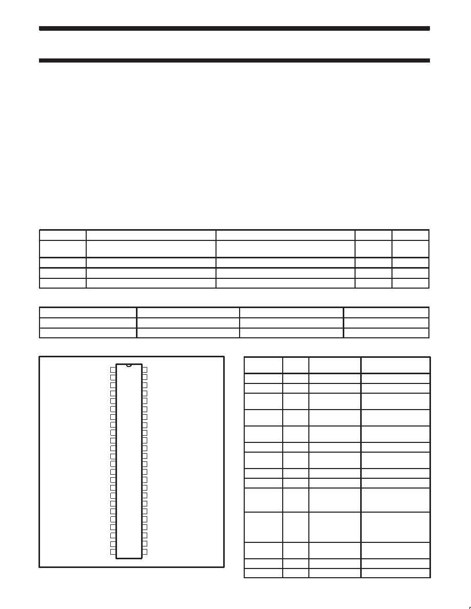
PIN CONFIGURATION
1
2
3
4
5
6
7
8
9
10
11
12
13
14
15
16
17
18
19
20
25
26
27
28
29
30
31
32
33
34
35
36
37
38
39
40
21
22
23
24
41
42
43
44
45
46
47
48
RESERVED
VDD0
BUF_OUT0
BUF_OUT1
VSS0
VDD1
BUF_OUT3
BUF_OUT2
VSS1
BUF_IN
VDD2
BUF_OUT4
BUF_OUT5
VSS2
VDD3
BUF_OUT6
BUF_OUT7
VSS3
VDD4
BUF_OUT16
VSS4
VDDI2C
SDA
RESERVED
VDD9
BUF_OUT15
BUF_OUT14
VSS9
VDD8
BUF_OUT13
BUF_OUT12
VSS8
OE
VDD7
BUF_OUT11
BUF_OUT10
VSS7
VDD6
BUF_OUT9
BUF_OUT8
VSS6
VDD5
BUF_OUT17
VSS5
VSSI2C
SCL
SW00731
PCK2002
I2C is a trademark of Philips Semiconductors Corporation.
PIN DESCRIPTION
PIN
NUMBER
I/O
TYPE
SYMBOL
FUNCTION
4, 5, 8, 9
Output
BUF_OUT (0–3)
Buffered clock outputs
13, 14, 17, 18
Output
BUF_OUT (4–7)
Buffered clock outputs
31, 32, 35,
36
Output
BUF_OUT
(8–11)
Buffered clock outputs
40, 41, 44,
45
Output
BUF_OUT
(12–15)
Buffered clock outputs
21, 28
Output
BUF_OUT
(16–17)
Buffered clock outputs
11
Input
BUF_IN
Buffered clock input
38
Input
OE
Active high output
enable
24
I/O
SDA
I2C serial data
25
Input
SCL
I2C serial clock
3, 7, 12, 16,
20, 29, 33,
37, 42, 46
Input
VDD (0–9)
3.3 V Power supply
6, 10, 15,
19, 22,
27, 30, 34,
39, 43
Input
VSS (0–9)
Ground
23
Input
VDDI2C
3.3 V I2C Power
supply
26
Input
VSSI2C
I2C Ground
1, 2, 47, 48
n/a
RESERVED
Undefined
相關(guān)PDF資料 |
PDF描述 |
|---|---|
| 935269807112 | LOW SKEW CLOCK DRIVER, 18 TRUE OUTPUT(S), 0 INVERTED OUTPUT(S), PDSO48 |
| 935269846112 | 200 MHz, PROC SPECIFIC CLOCK GENERATOR, PDSO48 |
| 935269848112 | LOW SKEW CLOCK DRIVER, 10 TRUE OUTPUT(S), 0 INVERTED OUTPUT(S), PDSO28 |
| 935269817118 | LOW SKEW CLOCK DRIVER, 10 TRUE OUTPUT(S), 0 INVERTED OUTPUT(S), PDSO28 |
| 935269971118 | LOW SKEW CLOCK DRIVER, 4 TRUE OUTPUT(S), 0 INVERTED OUTPUT(S), PDSO8 |
相關(guān)代理商/技術(shù)參數(shù) |
參數(shù)描述 |
|---|---|
| 935269987557 | 制造商:NXP Semiconductors 功能描述:SUB ONLY TDA9587-1US1-V1.8 SUBBED TO 935269987557 |
| 935270713557 | 制造商:NXP Semiconductors 功能描述:SUB ONLY IC CHP |
| 935270792551 | 制造商:NXP Semiconductors 功能描述:IC BUFF DVR TRI-ST 16BIT 56VFBGA |
| 935270792557 | 制造商:NXP Semiconductors 功能描述:IC BUFF DVR TRI-ST 16BIT 56VFBGA |
| 935270793551 | 制造商:NXP Semiconductors 功能描述:IC BUS TRCVR 3-ST 16BIT 56VFBGA |
發(fā)布緊急采購,3分鐘左右您將得到回復(fù)。