- 您現(xiàn)在的位置:買賣IC網(wǎng) > PDF目錄36339 > 935264467005 (NXP SEMICONDUCTORS) SPECIALTY CONSUMER CIRCUIT, UUC PDF資料下載
參數(shù)資料
| 型號: | 935264467005 |
| 廠商: | NXP SEMICONDUCTORS |
| 元件分類: | 消費(fèi)家電 |
| 英文描述: | SPECIALTY CONSUMER CIRCUIT, UUC |
| 封裝: | WAFER |
| 文件頁數(shù): | 22/24頁 |
| 文件大小: | 341K |
| 代理商: | 935264467005 |
1 Chip Specification
Rev. 2.2
January 2005
SL044022.doc/B
Public
Page 7 of 24
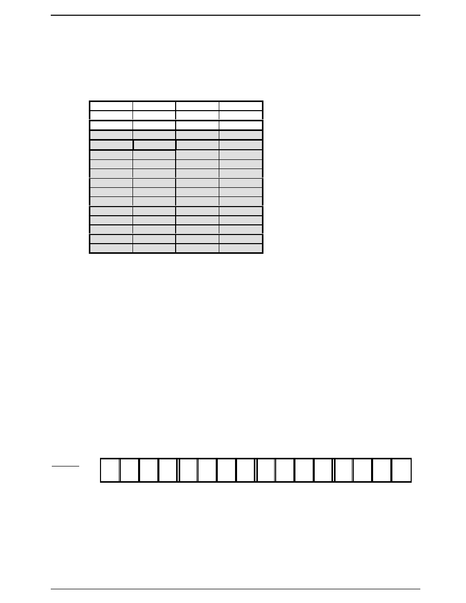
5.3 Memory Organisation
The 512 bit EEPROM memory is divided into 16 blocks. A block is the smallest access unit. Each
block consists of 4 bytes (1 block = 32 bits). Bit 0 in each byte represents the least significant bit
(LSB) and bit 7 the most significant bit (MSB), respectively.
Byte 0
Byte 1
Byte 2
Byte 3
Block 0
SNR0
SNR1
SNR2
SNR3
Serial Number (lower bytes)
Block 1
SNR4
SNR5
SNR6
SNR7
Serial Number (higher bytes)
Block 2
F0
FF
Write Access Conditions
Block 3
x
Special Functions (EAS/QUIET)
Block 4
x
Family Code/Application Identifier/User Data
Block 5
x
User Data
Block 6
x
:
Block 7
x
:
Block 8
x
:
Block 9
x
:
Block 10
x
:
Block 11
x
:
Block 12
x
:
Block 13
x
:
Block 14
x
:
Block 15
x
User Data
The values (in hexadecimal notation) shown in the table above are stored in the EEPROM after the
wafer production process. The contents of blocks marked with ‘x’ in the table are not defined at
delivery.
5.3.1 Serial Number
The unique 64 bit serial number is stored in blocks 0 and 1 and is programmed during the
production process. SNR0 in the table represents the least significant byte and SNR7 the most
significant byte, respectively.
5.3.2 Write Access Conditions
The Write Access Condition bits in block 2 determine the write access conditions for each of the
16 blocks. These bits can be set only to 0 (and never be changed to 1), i.e. already write protected
blocks can never be written to from this moment on. This is also true for block 2. If this block is set
into write protected state by clearing of bits 4 and 5 at byte 0, no further changes in write access
conditions are possible.
Byte 0
Byte 1
Byte 2
Byte 3
MSB
LSB
MSB
LSB
MSB
LSB
MSB
LSB
Block 2:
Write Access
Conditions
|
1|1
|
1|1
|
0
|0
|
0
|0
|
1|1
|
1|1
|
1|1
|
1|1
|
1|1
|
1|1
|
1|1
|
1|1
|
1|1
|
1|1
|
1|1
|
1|1
|
for Block
à
3
2
1
0
7
6
5
4
11
10
9
8
15
14
13
12
Special
Funct.
Write
Access
Serial
Number
User
Data
..... ..... ..... ..... ..... ..... ..... ..... ..... ..... User
Data
The ones in the 16 pairs of bits have to be cleared together if the corresponding block is wanted to
be write protected forever (1|1 à write access enabled, 0|0 à write access disabled). Writing of bit
pairs 1|0 or 0|1 to block 2 is not allowed!
It is extremely important to be particularly careful when clearing the Write Access bits in
block 2, as you can lose write access to all of the blocks on the label in case of a mistake.
Of course you can use this feature to put the label into a hardware write protected state!
相關(guān)PDF資料 |
PDF描述 |
|---|---|
| 935264530157 | SPECIALTY CONSUMER CIRCUIT, PQFP100 |
| 935264533557 | SPECIALTY CONSUMER CIRCUIT, PQFP100 |
| 935264539557 | SPECIALTY CONSUMER CIRCUIT, PQFP100 |
| 935266871557 | SPECIALTY CONSUMER CIRCUIT, PBGA292 |
| 935266917557 | SPECIALTY CONSUMER CIRCUIT, PBGA292 |
相關(guān)代理商/技術(shù)參數(shù) |
參數(shù)描述 |
|---|---|
| 935267356112 | 制造商:NXP Semiconductors 功能描述:IC TEA1507PN |
| 935268081112 | 制造商:NXP Semiconductors 功能描述:SUB ONLY IC |
| 935268721125 | 制造商:NXP Semiconductors 功能描述:Buffer/Line Driver 1-CH Non-Inverting 3-ST CMOS 5-Pin TSSOP T/R |
| 935269304128 | 制造商:ST-Ericsson 功能描述:IC AUDIO CODEC W/TCH SCRN 48LQFP |
| 935269544557 | 制造商:NXP Semiconductors 功能描述:SUB ONLY TDA9587-2US1-V1.3 |
發(fā)布緊急采購,3分鐘左右您將得到回復(fù)。