- 您現(xiàn)在的位置:買賣IC網(wǎng) > PDF目錄24809 > 935262899118 (NXP SEMICONDUCTORS) 8 I/O, PIA-GENERAL PURPOSE, PDSO16 PDF資料下載
參數(shù)資料
| 型號: | 935262899118 |
| 廠商: | NXP SEMICONDUCTORS |
| 元件分類: | 微控制器/微處理器 |
| 英文描述: | 8 I/O, PIA-GENERAL PURPOSE, PDSO16 |
| 封裝: | PLASTIC, TSSOP-16 |
| 文件頁數(shù): | 8/14頁 |
| 文件大?。?/td> | 144K |
| 代理商: | 935262899118 |
Philips Semiconductors
Product specification
PCA9556
Octal SMBus Registered Interface
1998 Dec 18
3
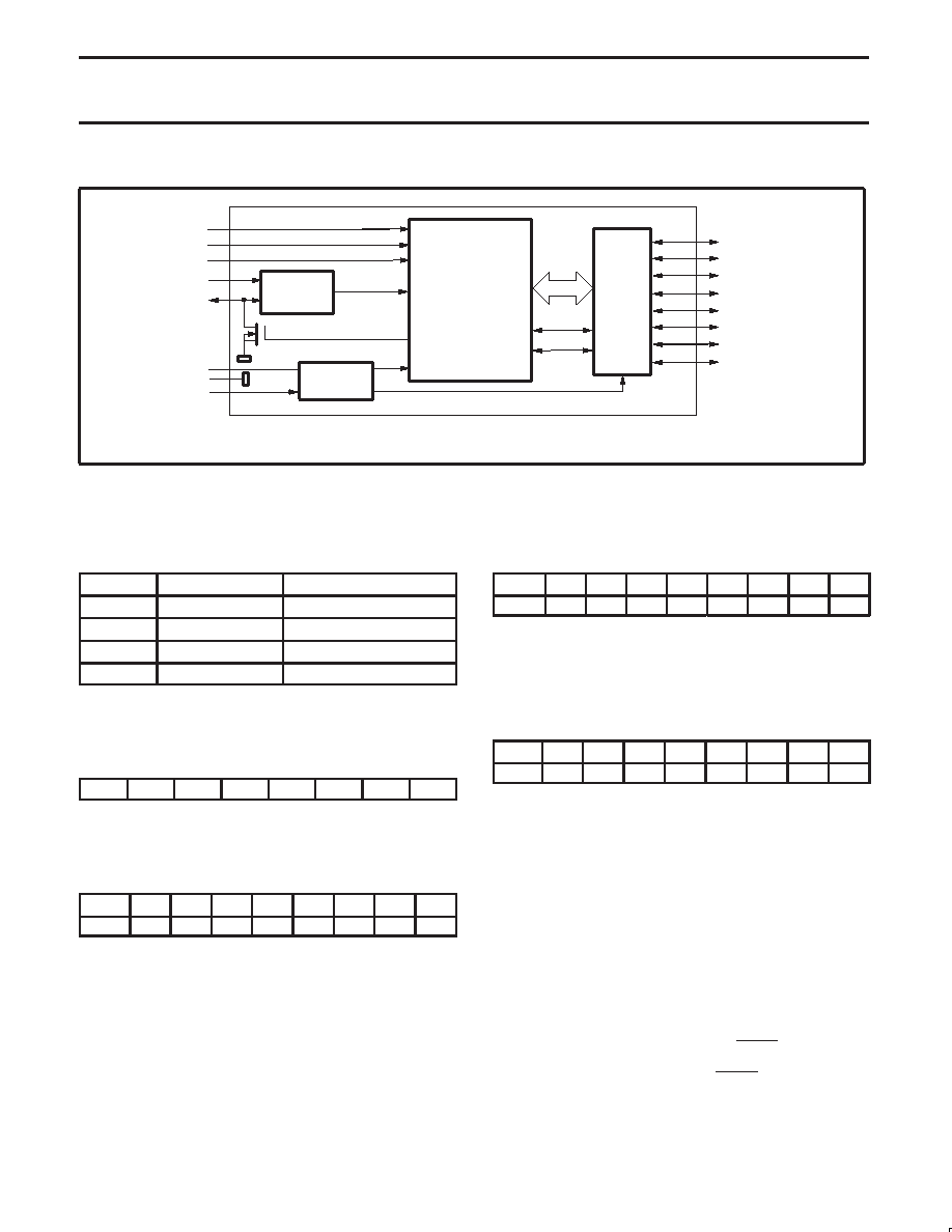
BLOCK DIAGRAM
POWER-
ON
RESET
INPUT
FILTER
SMBUS
CONTROL
INPUT/
OUT-
PUT
PORTS
WRITE pulse
READ pulse
A0
A1
A2
SCL
SDA
VDD
VSS
8-BIT
I/O0
I/O1
I/O2
I/O3
I/O4
I/O5
I/O6
I/O7
su01046
RESET
NOTE: ALL I/Os ARE SET TO INPUTS AT RESET
Figure 2. Block diagram
REGISTERS
Command Byte
Command
Protocol
Function
0
Read byte
Input port register
1
Read/write byte
Output port register
2
Read/write byte
Polarity inversion register
3
Read/write byte
I/O configuration register
The command byte is the first byte to follow the address byte during
a write transmission. It is used as a pointer to determine which of the
following registers will be written or read.
Register 0 – Input Port Register
I7
I6
I5
I4
I3
I2
I1
I0
This register is an input-only port. It reflects the incoming logic levels
of the pins, regardless of whether the pin is defined as an input or an
output by register 3. Writes to this register have no effect.
Register 1 – Output Port Register
bit
O7
O6
O5
O4
O3
O2
O1
O0
default
0
This register is an output-only port. It reflects the outgoing logic
levels of the pins defined as outputs by register 3. Bit values in this
register have no effect on pins defined as inputs. In turn, reads from
this register reflect the value that is in the flip-flop controlling the
output selection, NOT the actual pin value.
Register 2 – Polarity Inversion Register
bit
N7
N6
N5
N4
N3
N2
N1
N0
default
1
0
This register enables polarity inversion of pins defined as inputs by
register 3. If a bit in this register is set (written with ‘1’), the
corresponding port pin’s polarity is inverted. If a bit in this register is
cleared (written with a ‘0’), the corresponding port pin’s original
polarity is retained.
Register 3 – Input/Output Configuration Register
bit
C7
C6
C5
C4
C3
C2
C1
C0
default
1
This register configures the directions of the I/O pins. If a bit in this
register is set (written with ‘1’), the corresponding port pin is enabled
as an input with high impedance output driver. If a bit in this register
is cleared (written with ‘0’), the corresponding port pin is enabled as
an output.
RESET
Power-on Reset
When power is applied to VDD, an internal power-on reset holds the
PCA9556 in a reset state until VDD has reached VPOR. At that point,
the reset condition is released and the PCA9556 registers and
SMBus state machine will initialize to their default states.
External Reset
A reset can be accomplished by holding the RESET pin low for a
minimum of TW. The PCA9556 registers and SMBus state machine
will be held in their default state until the RESET input is once again
high. This input contains an internal pull-up, therefore, it may be left
open if not used.
相關(guān)PDF資料 |
PDF描述 |
|---|---|
| 935262900112 | PLL BASED CLOCK DRIVER, 10 TRUE OUTPUT(S), 0 INVERTED OUTPUT(S), PDSO48 |
| 935262900118 | PLL BASED CLOCK DRIVER, 10 TRUE OUTPUT(S), 0 INVERTED OUTPUT(S), PDSO48 |
| 935263011112 | SPECIALTY TELECOM CIRCUIT, PDSO16 |
| 935263011118 | SPECIALTY TELECOM CIRCUIT, PDSO16 |
| 935263040118 | AHC SERIES, HEX 1-INPUT INVERT GATE, PDSO14 |
相關(guān)代理商/技術(shù)參數(shù) |
參數(shù)描述 |
|---|---|
| 935264217557 | 制造商:NXP Semiconductors 功能描述:SUB ONLY IC |
| 935267356112 | 制造商:NXP Semiconductors 功能描述:IC TEA1507PN |
| 935268081112 | 制造商:NXP Semiconductors 功能描述:SUB ONLY IC |
| 935268721125 | 制造商:NXP Semiconductors 功能描述:Buffer/Line Driver 1-CH Non-Inverting 3-ST CMOS 5-Pin TSSOP T/R |
| 935269304128 | 制造商:ST-Ericsson 功能描述:IC AUDIO CODEC W/TCH SCRN 48LQFP |
發(fā)布緊急采購,3分鐘左右您將得到回復(fù)。