- 您現(xiàn)在的位置:買賣IC網(wǎng) > PDF目錄24664 > 933783430005 (NXP SEMICONDUCTORS) HC/UH SERIES, POSITIVE EDGE TRIGGERED D FLIP-FLOP, TRUE OUTPUT, UUC PDF資料下載
參數(shù)資料
| 型號: | 933783430005 |
| 廠商: | NXP SEMICONDUCTORS |
| 元件分類: | 鎖存器 |
| 英文描述: | HC/UH SERIES, POSITIVE EDGE TRIGGERED D FLIP-FLOP, TRUE OUTPUT, UUC |
| 封裝: | DIE |
| 文件頁數(shù): | 2/8頁 |
| 文件大小: | 56K |
| 代理商: | 933783430005 |
September 1993
2
Philips Semiconductors
Product specication
Octal D-type ip-op with reset;
positive-edge trigger
74HC/HCT273
FEATURES
Ideal buffer for MOS microprocessor or memory
Common clock and master reset
Eight positive edge-triggered D-type flip-flops
See “377” for clock enable version
See “373” for transparent latch version
See “374” for 3-state version
Output capability; standard
ICC category: MSI
GENERAL DESCRIPTION
The 74HC/HCT273 are high-speed Si-gate CMOS devices
and are pin compatible with low power Schottky TTL
(LSTTL). They are specified in compliance with JEDEC
standard no. 7A.
The 74HC/HCT273 have eight edge-triggered, D-type
flip-flops with individual D inputs and Q outputs. The
common clock (CP) and master reset (MR) inputs load and
reset (clear) all flip-flops simultaneously.
The state of each D input, one set-up time before the
LOW-to-HIGH clock transition, is transferred to the
corresponding output (Qn) of the flip-flop.
All outputs will be forced LOW independently of clock or
data inputs by a LOW voltage level on the MR input.
The device is useful for applications where the true output
only is required and the clock and master reset are
common to all storage elements.
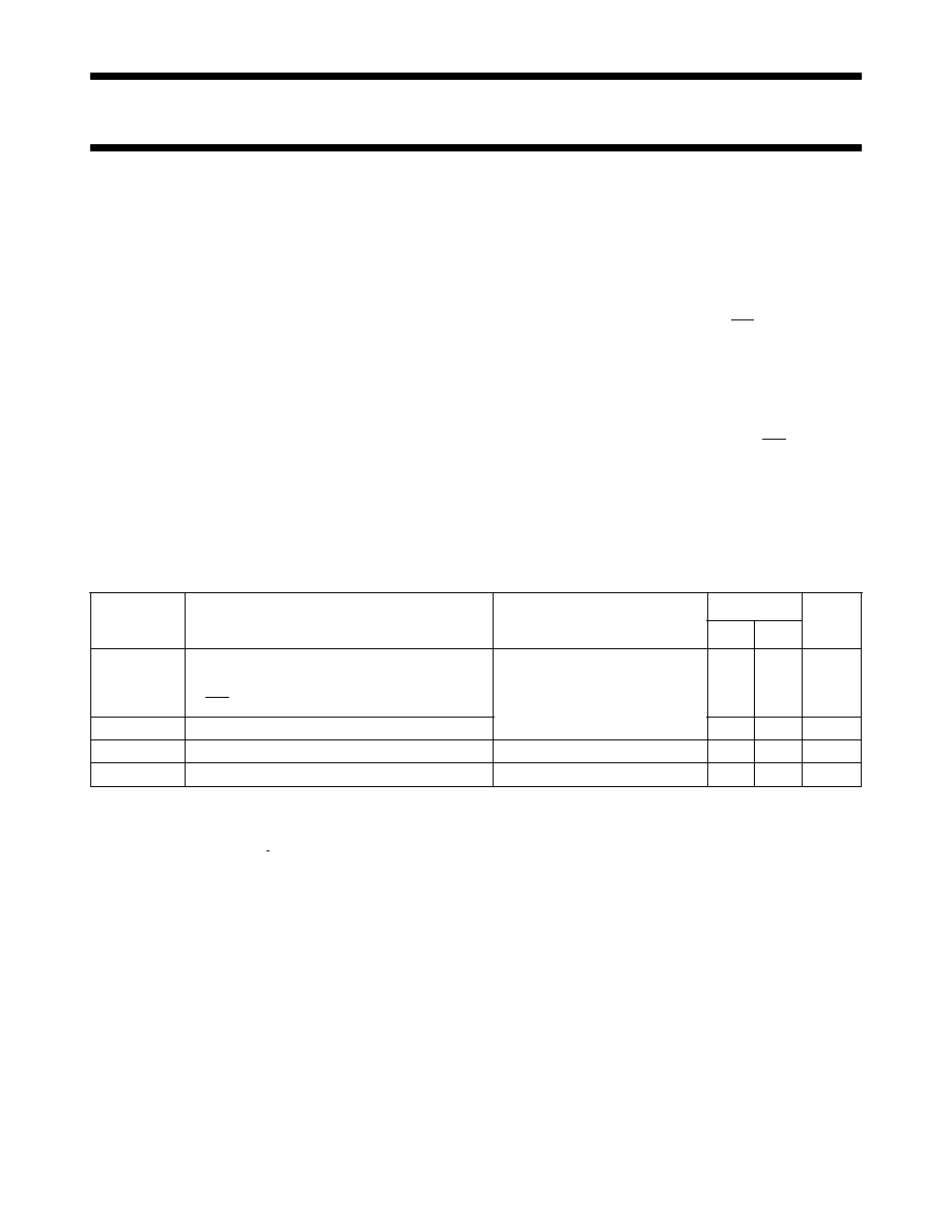
QUICK REFERENCE DATA
GND = 0 V; Tamb =25 °C; tr =tf = 6 ns
Notes
1. CPD is used to determine the dynamic power dissipation (PD in W):
PD =CPD × VCC2 × fi + ∑ (CL × VCC2 × fo) where:
fi = input frequency in MHz
fo = output frequency in MHz
∑ (CL × VCC2 × fo) = sum of outputs
CL = output load capacitance in pF
VCC = supply voltage in V
2. For HC the condition is VI = GND to VCC
For HCT the condition is VI = GND to VCC 1.5 V
ORDERING INFORMATION
See
“74HC/HCT/HCU/HCMOS Logic Package Information”.
SYMBOL
PARAMETER
CONDITIONS
TYPICAL
UNIT
HC
HCT
tPHL/ tPLH
propagation delay
CL = 15 pF; VCC =5 V
CP to Qn
15
ns
MR to Qn
15
20
ns
fmax
maximum clock frequency
66
36
MHz
CI
input capacitance
3.5
pF
CPD
power dissipation capacitance per flip-flop
notes 1 and 2
20
23
pF
相關(guān)PDF資料 |
PDF描述 |
|---|---|
| 935185830112 | HC/UH SERIES, POSITIVE EDGE TRIGGERED D FLIP-FLOP, TRUE OUTPUT, PDSO20 |
| 935183580112 | HCT SERIES, POSITIVE EDGE TRIGGERED D FLIP-FLOP, TRUE OUTPUT, PDSO20 |
| 933715440652 | HC/UH SERIES, POSITIVE EDGE TRIGGERED D FLIP-FLOP, TRUE OUTPUT, PDSO20 |
| 935174730112 | HC/UH SERIES, POSITIVE EDGE TRIGGERED D FLIP-FLOP, TRUE OUTPUT, PDSO20 |
| 933715440653 | HC/UH SERIES, POSITIVE EDGE TRIGGERED D FLIP-FLOP, TRUE OUTPUT, PDSO20 |
相關(guān)代理商/技術(shù)參數(shù) |
參數(shù)描述 |
|---|---|
| 9337-A17R | 制造商:GC Electronics 功能描述: |
| 9337C | 制造商:Hubbell Premise Wiring 功能描述: |
| 9337-CHR-100 | 制造商:Belden Inc 功能描述: |
| 9337CKE100M | 制造商:RFMD 制造商全稱:RF Micro Devices 功能描述:380W GaN WIDEBAND PULSED |
| 9337CMG | 制造商:Apex Tool Group 功能描述:7 IN. DIAGONAL CUTTING S J PLIERS W/CO-MOLDED GRIPS, LASER HARDENED EDGES, CDD |
發(fā)布緊急采購,3分鐘左右您將得到回復。