- 您現(xiàn)在的位置:買(mǎi)賣(mài)IC網(wǎng) > PDF目錄375093 > 7C185-12 (Cypress Semiconductor Corp.) 8K x 8 Static RAM PDF資料下載
參數(shù)資料
| 型號(hào): | 7C185-12 |
| 廠商: | Cypress Semiconductor Corp. |
| 英文描述: | 8K x 8 Static RAM |
| 中文描述: | 8K的× 8靜態(tài)RAM |
| 文件頁(yè)數(shù): | 1/11頁(yè) |
| 文件大?。?/td> | 197K |
| 代理商: | 7C185-12 |
8K x 8 Static RAM
CY7C185
Cypress Semiconductor Corporation
Document #: 38-05043 Rev. *A
3901 North First Street
San Jose
CA 95134
Revised September 13, 2002
408-943-2600
185
Features
High speed
—15 ns
Fast t
DOE
Low active power
—715 mW
Low standby power
—220 mW
CMOS for optimum speed/power
Easy memory expansion with CE
1
, CE
2
, and OE features
TTL-compatible inputs and outputs
Automatic power-down when deselected
Functional Description
[1]
The CY7C185 is a high-performance CMOS static RAM orga-
nized as 8192 words by 8 bits. Easy memory expansion is
provided by an active LOW chip enable (CE
1
), an active HIGH
chip enable (CE
2
), and active LOW output enable (OE) and
three-state drivers. This device has an automatic power-down
feature (CE
1
or CE
2
), reducing the power consumption by 70%
when deselected. The CY7C185 is in a standard 300-mil-wide
DIP, SOJ, or SOIC package.
An active LOW write enable signal (WE) controls the writ-
ing/reading operation of the memory. When CE
1
and WE in-
puts are both LOW and CE
2
is HIGH, data on the eight data
input/output pins (I/O
0
through I/O
7
) is written into the memory
location addressed by the address present on the address
pins (A
0
through A
12
). Reading the device is accomplished by
selecting the device and enabling the outputs, CE
1
and OE
active LOW, CE
2
active HIGH, while WE remains inactive or
HIGH. Under these conditions, the contents of the location ad-
dressed by the information on address pins are present on the
eight data input/output pins.
The input/output pins remain in a high-impedance state unless
the chip is selected, outputs are enabled, and write enable
(WE) is HIGH. A die coat is used to insure alpha immunity.
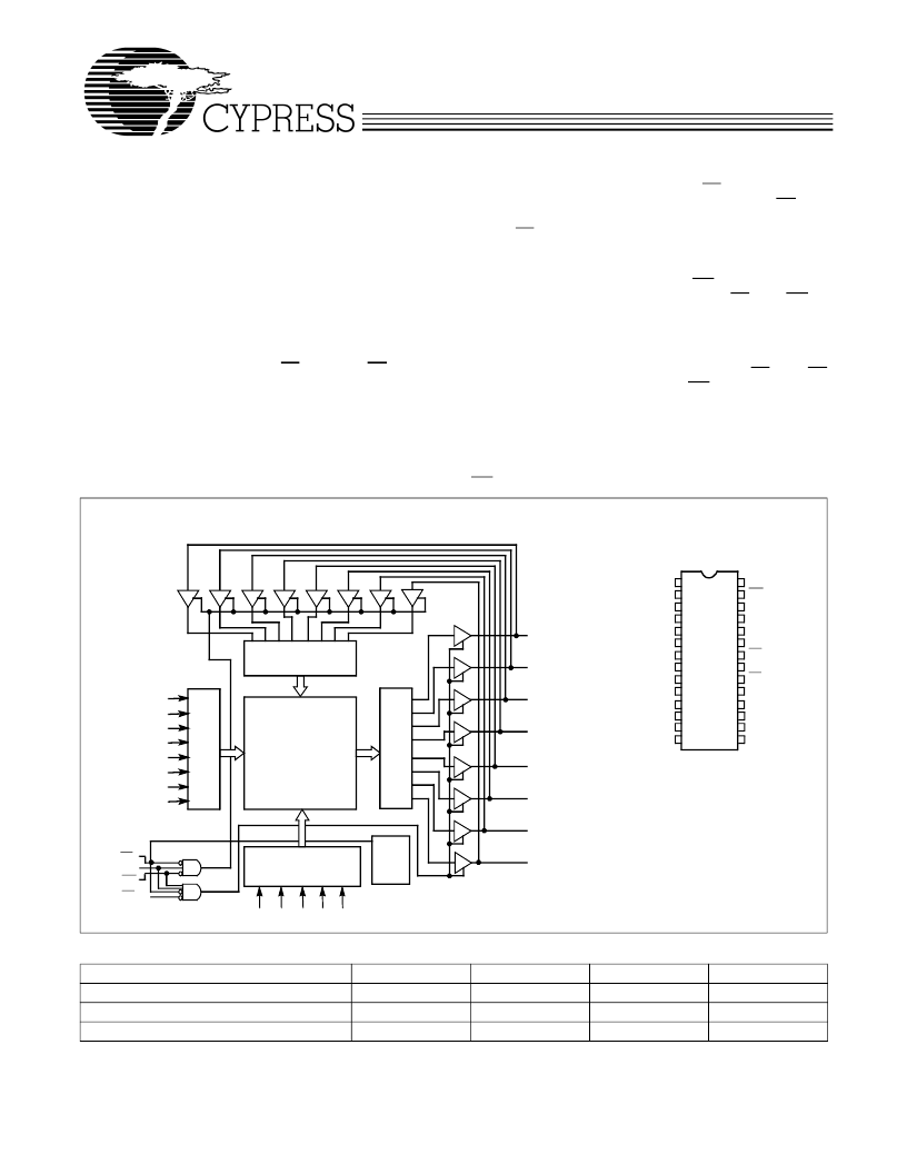
Logic Block Diagram
Pin Configurations
A
1
A
2
A
3
A
4
A
5
A
6
A
7
A
8
A
0
A
1
A
9
A
1
A
1
I/O
0
1
2
3
4
5
6
7
8
9
10
11
12
13
14
28
27
26
25
24
23
22
21
20
19
18
17
16
15
V
CC
WE
CE
2
A
3
A
2
A
1
OE
A
0
CE
1
I/O
7
I/O
6
I/O
5
I/O
4
I/O
3
NC
A
4
A
5
A
6
A
7
A
8
A
9
A
10
A
11
A
12
I/O
0
I/O
1
I/O
2
GND
256 x 32 x 8
ARRAY
INPUT BUFFER
COLUMN DECODER
R
S
POWER
DOWN
I/O
1
I/O
2
I/O
3
I/O
4
I/O
5
I/O
6
I/O
7
CE
1
CE
2
WE
OE
Top View
DIP/SOJ/SOIC
Selection Guide
[2]
7C185-15
15
130
40/15
7C185-20
20
110
20/15
7C185-25
25
100
20/15
7C185-35
35
100
20/15
Maximum Access Time (ns)
Maximum Operating Current (mA)
Maximum Standby Current (mA)
Note:
1.
For guidelines on SRAM system design, please refer to the
‘
System Design Guidelines
’
Cypress application note, available on the internet at www.cypress.com.
2.
For military specifications, see the CY7C185A data sheet.
相關(guān)PDF資料 |
PDF描述 |
|---|---|
| 7C185-15 | IC 16-BIT BUFF/LINE DRV 48 TSSOP |
| 7C185-20 | 8K x 8 Static RAM |
| 7C185-25 | 16-Bit Buffer/Line Driver |
| 7C185-35 | IC 16-BIT BUFF/LINE DVR 48-SSOP |
| 7C187-15 | 64K x 1 Static RAM |
相關(guān)代理商/技術(shù)參數(shù) |
參數(shù)描述 |
|---|---|
| 7C185-15 | 制造商:CYPRESS 制造商全稱(chēng):Cypress Semiconductor 功能描述:8K x 8 Static RAM |
| 7C185-20 | 制造商:CYPRESS 制造商全稱(chēng):Cypress Semiconductor 功能描述:8K x 8 Static RAM |
| 7C185-25 | 制造商:CYPRESS 制造商全稱(chēng):Cypress Semiconductor 功能描述:8K x 8 Static RAM |
| 7C185-35 | 制造商:CYPRESS 制造商全稱(chēng):Cypress Semiconductor 功能描述:8K x 8 Static RAM |
| 7C185-35VCT | 制造商:undefined 功能描述: |
發(fā)布緊急采購(gòu),3分鐘左右您將得到回復(fù)。