- 您現(xiàn)在的位置:買賣IC網(wǎng) > PDF目錄369357 > 7B991RPFS (MAXWELL TECHNOLOGIES) Programmable Skew Clock Buffer (PSCB) PDF資料下載
參數(shù)資料
| 型號: | 7B991RPFS |
| 廠商: | MAXWELL TECHNOLOGIES |
| 元件分類: | 時鐘及定時 |
| 英文描述: | Programmable Skew Clock Buffer (PSCB) |
| 中文描述: | PLL BASED CLOCK DRIVER, 8 TRUE OUTPUT(S), 0 INVERTED OUTPUT(S), DFP32 |
| 封裝: | RAD PAK, DFP-16 |
| 文件頁數(shù): | 6/17頁 |
| 文件大?。?/td> | 253K |
| 代理商: | 7B991RPFS |

M
6
All data sheets are subject to change without notice
2002 Maxwell Technologies.
All rights reserved.
Programmable Skew Clock Buffer (PSCB)
7B991
09.23.02 Rev 4
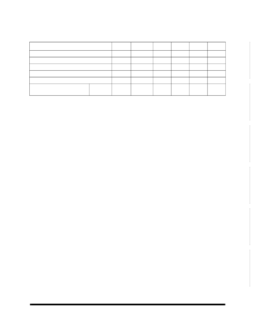
Output HIGH Time Deviation from50%
14,15
Output LOW Time Deviation from50%
14,15
Output Rise Time
14,16
Output Fall Time
14,16
PLL Lock Time
17
Cycle-to-Cycle Output Jitter
t
PWH
t
PWL
t
ORISE
t
OFALL
t
LOCK
t
JR
9, 10, 11
9, 10, 11
9, 10, 11
9, 10, 11
9, 10, 11
9, 10, 11
--
--
--
--
1.5
1.5
--
--
3
ns
ns
ns
ns
ms
ps
3.5
2.5
2.5
0.5
200
0.15
0.15
--
--
Peak-to-
Peak
3
1. The level to be set of FS in determned by the
“
normal
”
operating frequency (f
NOM
) of the V
CO
and Time Unit Generator (see
Logic Block Diagram. Nomnal frequency (f
NOM
) always appears at 1Q0 and the other outputs when they are operated in their
undivided modes (See Table 9). The frequency appearing at the REF and FB inputs will be f
NOM
when the output connected to
FB is undivided. The frequency of the REF and FB inputs will be f
NOM
/2 or f
NOM
/4 when the part is configured for a frequency
multiplication by using a divided output as the FB input.
2. Test measurement levels for the 7B991 are TTL levels (1.5V to 1.5V). Test conditions assume signal transition times of 2 ns or
less and output loading as shown in the AC Test Loads and Waveforms unless otherwise specified.
3. Guaranteed by statistical correlation. Tested initially and after any design or process changes that may affect these parameters.
4. For all three state inputs. HIGH indicates a connection to V
CC
, LOW indicates a connection to GND, and MID indicates an open
connections. Internal termnation circuitry holds an unconnected input to V
CC
/2.
5. When the FS pin is selected HIGH, the REF input must not transition upon power-up until V
CC
has reached 4.3V.
6. SKEW is defined as the time between the earliest and the latest output transition among all outputs for which the same t
U
delay
has been selected when all are loaded with 50 pF and termnated with 50
to 2.06V.
7. t
SKEWPR
is defined as the skew between a pair of outputs (XQ0 and XQ1) when all eight outputs are selected for 0t
U
.
8. t
SKEW0
is defined as the skew between outputs when they are selected for 0t
U
. Other outputs are divided or inverted but not
shifted.
9. C
L
= 0 pF. For C
L
= 30 pF, t
SKEW0
= 0.35 ns.
10.There are three classes of outputs: Nomnal (multiple of t
U
delay), Inverted (4Q0 and 4Q1 only with 4F0 = 4F1 = HIGH), and
divided (3Qx and 4Qx only in Divide-by-2 or Divide-by-4 mode).
11.t
DEV
is the output-to-output skew between any two devices operating under the same conditions (V
CC
ambient temperature, air
flow etc.)
12.Guaranteed by design.
13.t
ODCV
is the deviation of the output froma 50% duty cycle. Output pulse width variations are included in t
SKEW2
and t
SKEW4
spec-
ifications.
14.Specified with outputs loaded 30 pF for the 7B99 devices. Devices are termnated through 50
to 2.05V.
15.t
PWH
is measured at 2.0V. t
PWL
is measured at 0.8V.
16.t
ORISE
and t
OFALL
measured between 0.8V and 2.0V.
17.t
LOCK
is the time that is required before synchronization is achieved. This specification is valid only after V
CC
is stable and within
normal operating limts. This parameter is measured fromthe application of a new signal or frequency at REF or FB until t
PD
is
within specified limts.
T
ABLE
7. AC E
LECTRICAL
C
HARACTERISTICS
1,2,3
(V
CC
= 5V ±10%, T
A
= -40
TO
85
°
C,
UNLESS
OTHERWISE
SPECIFIED
)
S
YMBOL
P
ARAMETER
S
UBGROUPS
M
IN
T
YP
M
AX
U
NIT
相關(guān)PDF資料 |
PDF描述 |
|---|---|
| 7B991 | Programmable Skew Clock Buffer (PSCB) |
| 7BT2F9A-361 | HIGH CAPACITY ENVIRONMENTALLY SEALED |
| 7BT2 | HIGH CAPACITY ENVIRONMENTALLY SEALED |
| 7BT2F15A-361 | HIGH CAPACITY ENVIRONMENTALLY SEALED |
| 7BT2F15A-362 | HIGH CAPACITY ENVIRONMENTALLY SEALED |
相關(guān)代理商/技術(shù)參數(shù) |
參數(shù)描述 |
|---|---|
| 7B991V-2JC | 制造商:Cypress Semiconductor 功能描述: |
| 7B991V-5JZC | 制造商:Cypress Semiconductor 功能描述: |
| 7B991V-7JXC | 制造商: 功能描述: 制造商:undefined 功能描述: |
| 7B991VT | 制造商:Cypress Semiconductor 功能描述: |
| 7B9920A-5SC | 制造商:Cypress Semiconductor 功能描述: |
發(fā)布緊急采購,3分鐘左右您將得到回復(fù)。