- 您現(xiàn)在的位置:買賣IC網(wǎng) > PDF目錄360485 > 74LV165PWDH (NXP SEMICONDUCTORS) 8-bit parallel-in/serial-out shift register PDF資料下載
參數(shù)資料
| 型號: | 74LV165PWDH |
| 廠商: | NXP SEMICONDUCTORS |
| 元件分類: | 通用總線功能 |
| 英文描述: | 8-bit parallel-in/serial-out shift register |
| 中文描述: | LV/LV-A/LVX/H SERIES, 8-BIT RIGHT PARALLEL IN SERIAL OUT SHIFT REGISTER, COMPLEMENTARY OUTPUT, PDSO16 |
| 文件頁數(shù): | 7/14頁 |
| 文件大?。?/td> | 137K |
| 代理商: | 74LV165PWDH |
Philips Semiconductors
Product specification
74LV165
8-bit parallel-in/serial-out shift register
1998 May 07
7
AC CHARACTERISTICS
(
Continued
)
GND = 0V; t
r
= t
f
≤
2.5ns; C
L
= 50pF; R
L
= 1K
SYMBOL
PARAMETER
WAVEFORM
CONDITION
V
CC
(V)
1.2
–40 to +85
°
C
TYP
1
–40 to +125
°
C
MIN
UNIT
MIN
MAX
MAX
–
25
–
–
–
2.0
22
8
–
26
–
t
su
Set-up time
D
n
to PL
Figures 1, 2
2.7
16
6
–
19
–
ns
3.0 to 3.6
13
5
2
–
15
–
4.5 to 5.5
9
4
–
10
–
1.2
–
20
–
–
–
Hold time
D
to CP, CE
D to PL
2.0
22
7
–
26
–
t
h
Figures 1, 2
2.7
16
5
–
19
–
ns
3.0 to 3.6
13
4
–
15
–
4.5 to 5.5
9
3
–
10
–
1.2
–
–30
–
–
–
Hold time
CE to CP,
CP t CE
CP to CE
2.0
5
–8
–
5
–
t
h
Figures 1, 2
2.7
5
–6
–5
2
–
5
–
ns
3.0 to 3.6
5
–
5
–
4.5 to 5.5
5
–4
–
5
–
2.0
14
40
–
12
–
f
max
Maximum clock
pulse frequency
Figures 1 2
Figures 1, 2
2.7
19
60
65
2
75
–
16
–
MHz
3.0 to 3.6
4.5 to 5.5
24
36
–
–
20
30
–
–
NOTES:
1. Unless otherwise stated, all typical values are measured at T
amb
= 25
°
C
2. Typical values are measured at V
CC
= 3.3 V.
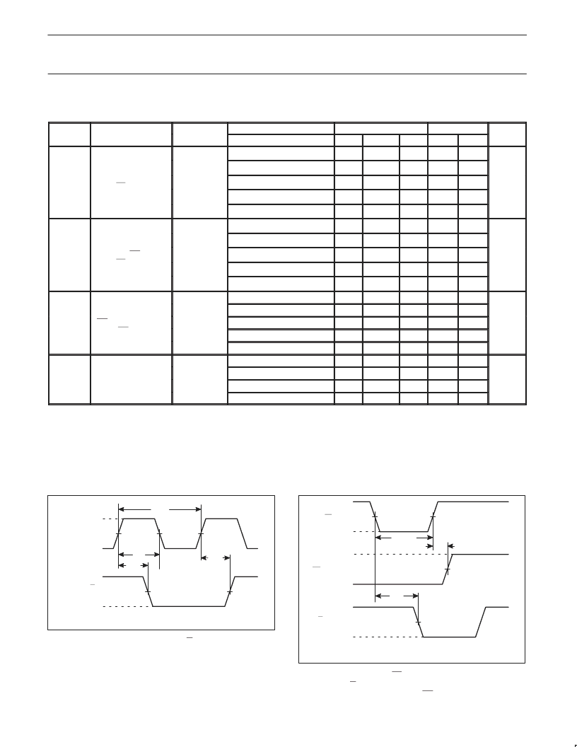
AC WAVEFORMS
V
M
= 1.5 V at V
CC
≥
2.7 V.
V
M
= 0.5
×
V
CC
at V
CC
<
2.7 V;
V
OL
and V
OH
are the typical output voltage drop that occur with the
output load.
SV00590
V
M
CP INPUT
V
I
GND
V
OH
V
OL
Q
7
or Q
7
OUTPUT
V
M
t
PLH
t
PHL
t
W
1/f
max
The changing to output assumes internal Q
6
opposite state from Q
7
.
Figure 1. Clock (CP) to output (Q
7
or Q
7
) propagation delays,
the clock pulse width and the maximum clock frequency.
Note to Figures 1 and 2
The changing to output assumes internal Q
6
opposite state from Q
7
.
SV00591
V
M
PL INPUT
CE, CP INPUT
V
I
V
I
GND
GND
V
OL
V
OH
Q
7
or Q
7
OUTPUT
V
M
V
M
t
rem
t
PHL
t
W
The changing to output assumes internal Q
6
opposite state from Q
7
.
Figure 2. Parallel load (PL) pulse width, the parallel load to
output (Q
7
or Q
7
) propagation delays, the parallel load to clock
(CP) and clock enable (CE) removal time.
相關PDF資料 |
PDF描述 |
|---|---|
| 74LV165 | 8-bit parallel-in/serial-out shift register(8位并入串出移位寄存器) |
| 74LV174 | Hex D-type flip-flop with reset;positive-edge trigger(上升沿觸發(fā),帶復位的六D觸發(fā)器) |
| 74LV174PWDH | Hex D-type flip-flop with reset; positive-edge trigger |
| 74LV175 | Quad D-type flip-flop with reset;positive-edge trigger(上升沿觸發(fā),帶復位的四D觸發(fā)器) |
| 74LV20PW | Dual 4-input NAND gate |
相關代理商/技術參數(shù) |
參數(shù)描述 |
|---|---|
| 74LV165PW-Q100J | 制造商:NXP Semiconductors 功能描述:74LV165PW-Q100/TSSOP16/REEL13/ - Tape and Reel 制造商:NXP Semiconductors 功能描述:IC SHIFT REGISTER 8BIT 16TSSOP |
| 74LV165PW-T | 功能描述:計數(shù)器移位寄存器 PRLLEL-LOAD 8BIT S/R RoHS:否 制造商:Texas Instruments 計數(shù)器類型: 計數(shù)順序:Serial to Serial/Parallel 電路數(shù)量:1 封裝 / 箱體:SOIC-20 Wide 邏輯系列: 邏輯類型: 輸入線路數(shù)量:1 輸出類型:Open Drain 傳播延遲時間:650 ns 最大工作溫度:+ 125 C 最小工作溫度:- 40 C 封裝:Reel |
| 74LV174 | 制造商:PHILIPS 制造商全稱:NXP Semiconductors 功能描述:Hex D-type flip-flop with reset; positive-edge trigger |
| 74LV174A | 制造商:TI 制造商全稱:Texas Instruments 功能描述:HEX D-TYPE FLIP-FLOPS WITH CLEAR |
| 74LV174D | 功能描述:觸發(fā)器 HEX D-TYPE MASTER RESET RoHS:否 制造商:Texas Instruments 電路數(shù)量:2 邏輯系列:SN74 邏輯類型:D-Type Flip-Flop 極性:Inverting, Non-Inverting 輸入類型:CMOS 輸出類型: 傳播延遲時間:4.4 ns 高電平輸出電流:- 16 mA 低電平輸出電流:16 mA 電源電壓-最大:5.5 V 最大工作溫度:+ 85 C 安裝風格:SMD/SMT 封裝 / 箱體:X2SON-8 封裝:Reel |
發(fā)布緊急采購,3分鐘左右您將得到回復。