- 您現(xiàn)在的位置:買賣IC網(wǎng) > PDF目錄360437 > 74F5302 (NXP Semiconductors N.V.) Fiber Optic Dual LED/clock Driver(光纖雙路LED/時(shí)鐘驅(qū)動(dòng)器) PDF資料下載
參數(shù)資料
| 型號: | 74F5302 |
| 廠商: | NXP Semiconductors N.V. |
| 英文描述: | Fiber Optic Dual LED/clock Driver(光纖雙路LED/時(shí)鐘驅(qū)動(dòng)器) |
| 中文描述: | 光纖雙LED /時(shí)鐘驅(qū)動(dòng)器(光纖雙路發(fā)光/時(shí)鐘驅(qū)動(dòng)器) |
| 文件頁數(shù): | 4/10頁 |
| 文件大小: | 81K |
| 代理商: | 74F5302 |
Philips Semiconductors
Product specification
74F5302
Fiber optic dual LED/clock driver
July 24, 1990
4
DC ELECTRICAL CHARACTERISTICS
(Over recommended operating free-air temperature range unless otherwise noted.)
SYMBOL
PARAMETER
TEST CONDITIONS
1
LIMITS
TYP
2
UNIT
MIN
MAX
V
CC
= MIN,
±
10%V
CC
±
5%V
CC
V
CC
= 5V
2.5
V
V
OH
High-level output voltage
V
IL
= MAX,
I
OH
= –80mA
2.8
3.3
3.9
V
V
IH
= MIN
3.0
3.3
3.6
V
I
OH
= –160mA
±
10%V
CC
2.0
V
V
CC
= MIN,
I
OL
= 100mA
±
10%V
CC
±
10%V
CC
±
10%V
CC
0.42
0.55
V
V
OL
Low-level output voltage
V
IL
= MAX,
I
OL
= 120mA
0.45
0.60
V
V
IH
= MIN
I
OL
= 160mA
0.55
0.80
V
V
IK
I
I
I
IH
I
IL
I
CC
Input clamp voltage
V
CC
= MIN, I
I
= I
IK
V
CC
= MAX, V
I
= 7.0V
V
CC
= MAX, V
I
= 2.7V
V
CC
= MAX, V
I
= 0.5V
V
CC
= MAX
V
CC
= MAX
-0.73
-1.2
V
μ
A
Input current at maximum input voltage
100
High–level input current
20
μ
A
Low–level input current
-0.6
mA
Supply current (total)
I
CCH
I
CCL
5.0
12
mA
18
25
mA
NOTES:
1. For conditions shown as MIN or MAX, use the appropriate value specified under recommended operating conditions for the applicable type.
2. All typical values are at V
CC
= 5V, T
amb
= 25
°
C.
3. The device is not short circuit protected.
AC ELECTRICAL CHARACTERISTICS
LIMITS
T
amb
= +25
°
C
V
CC
= +5.0V
C
L
= 50pF, R
L
= 100
MIN
TYP
T
amb
= 0
°
C to +70
°
C
V
CC
= +5.0V
±
10%
C
L
= 50pF, R
L
= 100
MIN
SYMBOL
PARAMETER
TEST CONDITION
UNIT
MAX
MAX
t
PLH
t
PHL
D
tpw
t
RFS
t
sk (0)
t
THL
t
TLH
NOTES:
1. D
tpw
is defined as the difference between input pulse width and output pulse width (0 to 3 volt swing and 50% duty cycle).
2. | t
PN
actual – t
PM
actual| for any output compared to any other output where N and M are either LH or HL.
3. | t
TLH
actual – t
THL
actual|.
4. Skew times are valid only under same test conditions (temperature, V
CC
, loading, etc.,).
Propagation delay
Dn, En
,
to Qn
Pulse width distortion
1
Rise and fall time skew
3, 4
Output skew
2,
4
Waveform 1
1.0
1.0
2.0
2.5
4.5
5.0
1.0
1.0
4.5
5.0
ns
Frequency = 10MHz
0.8
1.2
1.8
ns
0.3
1.5
2.0
ns
Waveform 2
0.9
1.3
1.6
ns
Fall time 90% to 10%
Rise time 10% to 90%
Test circuits and
Waveforms
1.0
1.0
1.5
1.8
3.0
3.0
0.5
0.5
4.0
4.5
ns
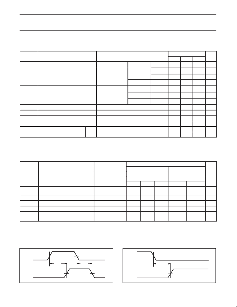
AC WAVEFORMS
V
M
V
M
V
M
V
M
Qn
Dn, En
t
PLH
t
PHL
SF00594
Waveform 1. Propagation delay for input to output
NOTE:
For all waveforms, V
M
= 1.5V.
V
M
V
M
Qn
t
sk (0)
Qn
SF00595
Waveform 2. Output skew
相關(guān)PDF資料 |
PDF描述 |
|---|---|
| 74F533DC | 8-Bit D-Type Latch |
| 74F533SCX | 8-Bit D-Type Latch |
| 74F533SJX | 8-Bit D-Type Latch |
| 74F534SCX | Octal D-Type Flip-Flop |
| 74F534SJX | Octal D-Type Flip-Flop |
相關(guān)代理商/技術(shù)參數(shù) |
參數(shù)描述 |
|---|---|
| 74F533 | 制造商:NSC 制造商全稱:National Semiconductor 功能描述:Octal Transparent Latch with TRI-STATE Outputs |
| 74F533_TKH3026B WAF | 制造商:Fairchild Semiconductor Corporation 功能描述: |
| 74F533DC | 制造商:未知廠家 制造商全稱:未知廠家 功能描述:8-Bit D-Type Latch |
| 74F533DCQB | 制造商:NSC 制造商全稱:National Semiconductor 功能描述:Octal Transparent Latch with TRI-STATE Outputs |
| 74F533DCX | 制造商:NSC 制造商全稱:National Semiconductor 功能描述:Octal Transparent Latch with TRI-STATE Outputs |
發(fā)布緊急采購,3分鐘左右您將得到回復(fù)。