- 您現(xiàn)在的位置:買(mǎi)賣(mài)IC網(wǎng) > PDF目錄360437 > 74F5302 (NXP Semiconductors N.V.) Fiber Optic Dual LED/clock Driver(光纖雙路LED/時(shí)鐘驅(qū)動(dòng)器) PDF資料下載
參數(shù)資料
| 型號(hào): | 74F5302 |
| 廠商: | NXP Semiconductors N.V. |
| 英文描述: | Fiber Optic Dual LED/clock Driver(光纖雙路LED/時(shí)鐘驅(qū)動(dòng)器) |
| 中文描述: | 光纖雙LED /時(shí)鐘驅(qū)動(dòng)器(光纖雙路發(fā)光/時(shí)鐘驅(qū)動(dòng)器) |
| 文件頁(yè)數(shù): | 2/10頁(yè) |
| 文件大小: | 81K |
| 代理商: | 74F5302 |
Philips Semiconductors
Product specification
74F5302
Fiber optic dual LED/clock driver
2
July 24, 1990
853-1410 00037
FEATURES
TTL inputs
Output enable control
High current source and sink capability
Matched propagation delay times (t
PLH
, t
PHL
)
Symmetrical rise and fall times
ESD protection greater than 2000 volts
Single +5V supply
Surface mount package
APPLICATIONS
High speed serial data communication
Fiber optic data links
Local area and metropolitan area networks
Digital Television
PBX systems
ASSOCIATED PRODUCTS
NE5210/11/12 transimpedance amplifiers
NE5214/5217 postamplifiers with link status indicator
74F5300 fiber optic LED driver
TYPE
TYPICAL
PROPAGATION
DELAY
TYPICAL SUPPLY
CURRENT( TOTAL)
74F5302
2.5ns
8mA
ORDERING INFORMATION
ORDER CODE
DESCRIPTION
COMMERCIAL RANGE
V
CC
= 5V
±
10%,
T
amb
= 0
°
C to +70
°
C
N74F5302N
PKG DWG #
14–pin plastic DIP
SOT27-1
14–pin plastic SO
N74F5302D
SOT108-1
INPUT AND OUTPUT LOADING
AND FAN OUT TABLE
PINS
DESCRIPTION
74F (U.L.)
HIGH/LOW
LOAD VALUE
HIGH/LOW
20
μ
A/0.6mA
20
μ
A/0.6mA
Dn
Data inputs
1.0/1.0
En
Enable inputs
1.0/1.0
Qn
Current driver output
8000/266.6
160mA/160mA
NOTE:
One (1.0) FAST unit load is defined as: 20
μ
A in the high
state and 0.6mA in the low state.
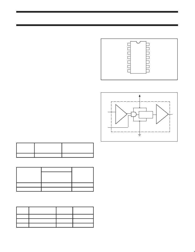
PIN CONFIGURATION
14
13
12
11
10
9
8
7
6
5
4
3
2
1
NC
V
CC
D1
E1
E0
NC
Q0
Q1
GND
GND
GND
D0
V
CC
V
CC
SF00591
LOGIC DIAGRAM (ONE DRIVER)
V
= Pin 10, 11, 12
GND = Pin 3, 4, 5
Linearizing
circuit
Output
driver
amp
TTL
input
buffer
D0
E0
14
13
2
Q0
V
CC
GND
SF00592
DESCRIPTION
The 74F5302 is a dual LED/clock driver designed for use in fiber
optic links. The 74F5302 is ideally suited for use in high speed
optical high transmitter systems. It is also ideal for use as a clock
driver.
The TTL input buffer accepts TTL data. The linearizing circuits
ensures a constant propagation delay for t
PLH
and t
PHL,
and controls
the rise and fall times. The output driver amplifier is capable of
sourcing more than 160mA and sinking more than 160mA at low
impedances. The high current output driver has been designed to
deal with transmission line effects of high speed switching systems
with fast rising and falling edges. The performance of the system
can be enhanced by matching impedance at the output for proper
termination. It exhibits closely matched propagation delays (t
PLH
and
t
PHL
) and symmetrical rise and fall times. The resulting optical
waveform has minimal duty cycle distortion (DCD). When used with
the external pre–bias and pre–charging circuits, the response can
be tailored to a specific LED to eliminate any overshoot and to
minimize the long fall response.
Additionally, this part can be used as the transmitter in a complete
fiber optic system when combined with any of the
NE5210/5211/5212 preamplifiers and NE5214/5217 postamplifiers
for the optical receiver. Please refer to applications note AN1121 in
the Philips Semiconductors Fiber Optic Communication Data Book
for more specific applications information.
相關(guān)PDF資料 |
PDF描述 |
|---|---|
| 74F533DC | 8-Bit D-Type Latch |
| 74F533SCX | 8-Bit D-Type Latch |
| 74F533SJX | 8-Bit D-Type Latch |
| 74F534SCX | Octal D-Type Flip-Flop |
| 74F534SJX | Octal D-Type Flip-Flop |
相關(guān)代理商/技術(shù)參數(shù) |
參數(shù)描述 |
|---|---|
| 74F533 | 制造商:NSC 制造商全稱(chēng):National Semiconductor 功能描述:Octal Transparent Latch with TRI-STATE Outputs |
| 74F533_TKH3026B WAF | 制造商:Fairchild Semiconductor Corporation 功能描述: |
| 74F533DC | 制造商:未知廠家 制造商全稱(chēng):未知廠家 功能描述:8-Bit D-Type Latch |
| 74F533DCQB | 制造商:NSC 制造商全稱(chēng):National Semiconductor 功能描述:Octal Transparent Latch with TRI-STATE Outputs |
| 74F533DCX | 制造商:NSC 制造商全稱(chēng):National Semiconductor 功能描述:Octal Transparent Latch with TRI-STATE Outputs |
發(fā)布緊急采購(gòu),3分鐘左右您將得到回復(fù)。