- 您現(xiàn)在的位置:買賣IC網(wǎng) > PDF目錄360435 > 74F382SC (FAIRCHILD SEMICONDUCTOR CORP) 4-Bit Arithmetic Logic Unit PDF資料下載
參數(shù)資料
| 型號(hào): | 74F382SC |
| 廠商: | FAIRCHILD SEMICONDUCTOR CORP |
| 元件分類: | 通用總線功能 |
| 英文描述: | 4-Bit Arithmetic Logic Unit |
| 中文描述: | F/FAST SERIES, 4-BIT ARITHMETIC LOGIC UNIT, PDSO20 |
| 封裝: | 0.300 INCH, MS-013, SOIC-20 |
| 文件頁數(shù): | 7/12頁 |
| 文件大小: | 121K |
| 代理商: | 74F382SC |
Philips Semiconductors
Product specification
74F382
Arithmetic logic unit
1990 Jul 12
7
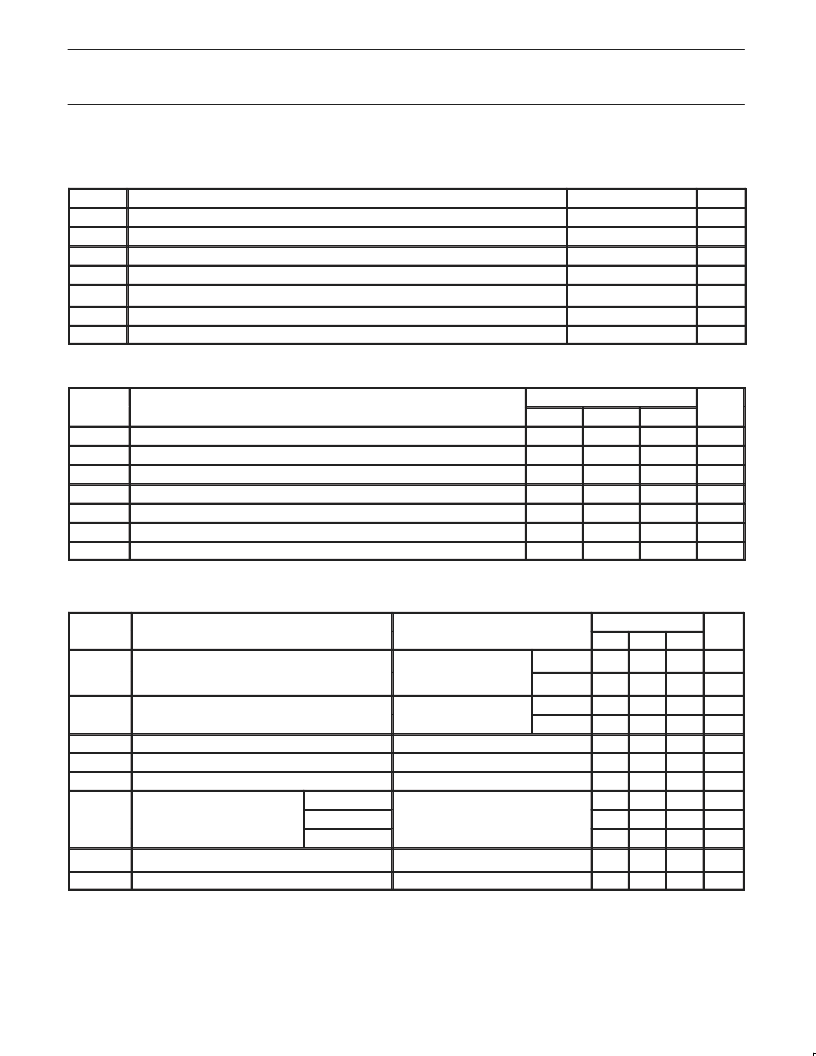
ABSOLUTE MAXIMUM RATINGS
(Operation beyond the limit set forth in this table may impair the useful life of the device. Unless otherwise noted these limits are over the
operating free-air temperature range.)
SYMBOL
PARAMETER
RATING
UNIT
V
CC
V
IN
I
IN
V
OUT
Supply voltage
–0.5 to +7.0
V
Input voltage
–0.5 to +7.0
V
Input current
–30 to +1
mA
Voltage applied to output in High output state
–0.5 to +V
CC
V
I
OUT
Current applied to output in Low output state
40
mA
T
amb
T
stg
Operating free-air temperature range
0 to +70
°
C
°
C
Storage temperature range
–65 to +150
RECOMMENDED OPERATING CONDITIONS
SYMBOL
PARMETER
LIMITS
UNIT
SYMBOL
MIN
NOM
MAX
V
CC
V
IH
V
IL
I
IK
I
OH
I
OL
T
amb
Supply voltage
4.5
5.0
5.5
V
High-level input voltage
2.0
V
Low-level input voltage
0.8
V
Input clamp current
–18
mA
High-level output current
–1
mA
Low-level output current
20
mA
Operating free-air temperature range
0
70
°
C
DC ELECTRICAL CHARACTERISTICS
(Over recommended operating free-air temperature range unless otherwise noted.)
SYMBOL
PARAMETER
TEST
LIMITS
TYP
2
UNIT
CONDITIONS
1
MIN
MAX
V
OH
High level output voltage
High-level output voltage
V
CC
= MIN, V
IL
= MAX,
±
10%V
CC
2.5
V
V
IH
= MIN, I
OH
= MAX
±
5%V
CC
2.7
3.4
V
V
OL
Low level output voltage
Low-level output voltage
V
CC
= MIN, V
IL
= MAX,
V
IH
= MIN, I
OL
= MAX
V
CC
= MIN, I
I
= I
IK
V
CC
= MAX, V
I
= 7.0V
V
CC
= MAX, V
I
= 2.7V
±
10%V
CC
±
5%V
CC
0.30
0.50
V
0.30
0.50
V
V
IK
I
I
I
IH
Input clamp voltage
–0.73
–1.2
V
μ
A
μ
A
Input current at maximum input voltage
100
High-level input current
20
Cn
–3.0
mA
I
IL
Low-level input current
A0–A3, B0–B3
V
CC
= MAX, V
I
= 0.5V
–2.4
mA
S0, S1, S2
–0.6
mA
I
OS
Short-circuit output current
3
V
CC
= MAX
–60
–150
mA
I
CC
Supply current (total)
V
CC
= MAX
54
81
mA
NOTES:
1. For conditions shown as MIN or MAX, use the appropriate value specified under recommended operating conditions for the applicable type.
2. All typical values are at V
CC
= 5V, T
amb
= 25
°
C.
3. Not more than one output should be shorted at a time. For testing I
OS
, the use of high-speed test apparatus and/or sample-and-hold
techniques are preferable in order to minimize internal heating and more accurately reflect operational values. Otherwise, prolonged shorting
of a High output may raise the chip temperature well above normal and thereby cause invalid readings in other parameter tests. In any
sequence of parameter tests, I
OS
tests should be performed last.
相關(guān)PDF資料 |
PDF描述 |
|---|---|
| 74F382SJ | 4-Bit Arithmetic Logic Unit |
| 74F382SCX | Fixed Point ALU |
| 74F382SJX | Fixed Point ALU |
| 74F385 | Quad serial adder/subtractor |
| 74F3893 | Quad Futurebus backplane transceiver(四通道預(yù)置總線底板收發(fā)器) |
相關(guān)代理商/技術(shù)參數(shù) |
參數(shù)描述 |
|---|---|
| 74F382SCX | 功能描述:算數(shù)邏輯單元 - ALU 4-Bit Arith Log Unit RoHS:否 制造商:ON Semiconductor 高電平輸出電流: 低電平輸出電流: 傳播延遲時(shí)間: 電源電壓-最大:18 V 電源電壓-最小:3 V 封裝 / 箱體:SOIC-16 Wide 最大工作溫度:+ 125 C 封裝:Reel |
| 74F382SJ | 功能描述:算數(shù)邏輯單元 - ALU 4-Bit Arith Log Unit RoHS:否 制造商:ON Semiconductor 高電平輸出電流: 低電平輸出電流: 傳播延遲時(shí)間: 電源電壓-最大:18 V 電源電壓-最小:3 V 封裝 / 箱體:SOIC-16 Wide 最大工作溫度:+ 125 C 封裝:Reel |
| 74F382SJX | 制造商:FAIRCHILD 制造商全稱:Fairchild Semiconductor 功能描述:Fixed Point ALU |
| 74F385 | 制造商:PHILIPS 制造商全稱:NXP Semiconductors 功能描述:Quad serial adder/subtractor |
| 74F3893 | 制造商:PHILIPS 制造商全稱:NXP Semiconductors 功能描述:Quad futurebus backplane transceiver |
發(fā)布緊急采購,3分鐘左右您將得到回復(fù)。