- 您現(xiàn)在的位置:買賣IC網(wǎng) > PDF目錄360348 > 74ABT161543DGG (NXP SEMICONDUCTORS) 16-bit latched transceiver with dual enable and master reset 3-State PDF資料下載
參數(shù)資料
| 型號(hào): | 74ABT161543DGG |
| 廠商: | NXP SEMICONDUCTORS |
| 元件分類: | 通用總線功能 |
| 英文描述: | 16-bit latched transceiver with dual enable and master reset 3-State |
| 中文描述: | ABT SERIES, DUAL 8-BIT REGISTERED TRANSCEIVER, TRUE OUTPUT, PDSO56 |
| 封裝: | PLASTIC, TSSOP2-56 |
| 文件頁(yè)數(shù): | 6/12頁(yè) |
| 文件大小: | 85K |
| 代理商: | 74ABT161543DGG |
Philips Semiconductors
Product specification
74ABT161543
74ABTH161543
16-bit latched transceiver with dual enable
and master reset (3-State)
1998 Feb 27
6
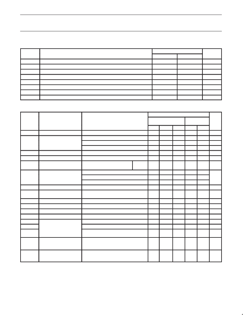
RECOMMENDED OPERATING CONDITIONS
SYMBOL
PARAMETER
LIMITS
UNIT
Min
4.5
0
2.0
Max
5.5
V
CC
V
CC
V
I
V
IH
V
IL
I
OH
I
OL
t/
v
T
amb
DC supply voltage
Input voltage
High-level input voltage
Low-level Input voltage
High-level output current
Low-level output current
Input transition rise or fall rate
Operating free-air temperature range
V
V
V
V
0.8
–32
64
10
+85
mA
mA
ns/V
°
C
0
–40
DC ELECTRICAL CHARACTERISTICS
LIMITS
SYMBOL
PARAMETER
TEST CONDITIONS
T
amb
= +25
°
C
T
amb
= –40
°
C
°
C
MIN
UNIT
MIN
TYP
MAX
–1.2
MAX
–1.2
V
IK
Input clamp voltage
V
CC
= 4.5V; I
IK
= –18mA
V
CC
= 4.5V; I
OH
= –3mA; V
I
= V
IL
or V
IH
V
CC
= 5.0V; I
OH
= –3mA; V
I
= V
IL
or V
IH
V
CC
= 4.5V; I
OH
= –32mA; V
I
= V
IL
or V
IH
V
CC
= 4.5V; I
OL
= 64mA; V
I
= V
IL
or V
IH
V
CC
= 5.5V; I
O
= 1mA; V
I
= GND or V
CC
V
V
V
V
V
V
2.5
3.0
2.0
3.0
3.6
2.7
0.36
0.13
2.5
3.0
2.0
V
OH
High-level output voltage
V
OL
V
RST
Low-level output voltage
Power-up output voltage
3
0.55
0.55
0.55
0.55
I
I
Input leakag
current
= 5 5V; V
= GND or 5 5V
V
CC
= 5.5V V
I
= GND or 5.5V
Control
pins
0 01
0.01
1 0
±
1.0
1 0
±
1.0
μ
A
Bus Hold current A or B
Ports 74ABTH161543
V
CC
= 4.5V; V
I
= 0.8V
V
CC
= 4.5V; V
I
= 2.0V
V
CC
= 5.5V; V
I
= 0 to 5.5V
V
CC
= 0.0V; V
O
or V
I
≤
4.5V
V
CC
= 2.1V; V
O
= 0.0V or V
CC
;
V
I
= GND or V
CC
; V
OE
= Don’t care
V
CC
= 5.5V; V
O
= 5.5V; V
I
= V
IL
or V
IH
V
CC
= 5.5V; V
O
= 0.0V; V
I
= V
IL
or V
IH
V
CC
= 5.5V; V
O
= 5.5V; V
I
= GND or V
CC
V
CC
= 5.5V; V
O
= 2.5V
V
CC
= 5.5V; Outputs High, V
I
= GND or V
CC
V
CC
= 5.5V; Outputs Low, V
I
= GND or V
CC
V
CC
= 5.5V; Outputs 3–State;
V
I
CC
35
–75
±
800
35
–75
I
HOLD
μ
A
I
OFF
Power-off leakage current
Power-up/down 3-State
output current
4
3-State output High current
3-State output Low current
Output High leakage current
Output current
1
1.0
±
100
±
100
μ
A
I
PU/PD
1.0
±
50
±
50
μ
A
I
IH
+ I
OZH
I
IL
+ I
OZL
I
CEX
I
O
I
CCH
I
CCL
1.0
–1.0
1.0
–100
0.50
9
50
–50
50
–200
1.5
19
50
–50
50
–200
1.5
19
μ
A
μ
A
μ
A
mA
mA
mA
–50
–50
Quiescent supply current
I
CCZ
0.50
1.5
1.5
mA
I
CC
Additional supply current
per input pin
2
74ABT161543
V
CC
= 5.5V; one input at 3.4V,
other inputs at V
CC
or GND
5.0
100
100
μ
A
I
CC
Additional supply current
per input pin
2
74ABTH161543
V
CC
= 5.5V; one input at 3.4V,
other inputs at V
CC
or GND
0.20
1
1
mA
NOTES:
1. Not more than one output should be tested at a time, and the duration of the test should not exceed one second.
2. This is the increase in supply current for each input at 3.4V.
3. For valid test results, data must not be loaded into the flip-flops (or latches) after applying the power.
4. This parameter is valid for any V
CC
between 0V and 2.1V, with a transition time of up to 10msec. From V
CC
= 2.1V to V
CC
= 5V
±
10% a
transition time of up to 100
μ
sec is permitted.
5. This is the bus hold overdrive current required to force the input to the opposite logic state.
相關(guān)PDF資料 |
PDF描述 |
|---|---|
| 74ABTH161543DGG | 16-bit latched transceiver with dual enable and master reset 3-State |
| 74ABT161543 | 16-bit latched transceiver with dual enable and master reset 3-State |
| 74ABT161543DL | 16-bit latched transceiver with dual enable and master reset 3-State |
| 74ABTH161543 | 16-Bit Latched Transceiver With Dual Enable and Master Reset (3-State)(帶雙路使能和主線復(fù)位的16位鎖存的收發(fā)器) |
| 74ABTH161543DL | 16-bit latched transceiver with dual enable and master reset 3-State |
相關(guān)代理商/技術(shù)參數(shù) |
參數(shù)描述 |
|---|---|
| 74ABT161543DG-T | 制造商:未知廠家 制造商全稱:未知廠家 功能描述:Dual 8-bit Bus Transceiver |
| 74ABT161543DL | 制造商:PHILIPS 制造商全稱:NXP Semiconductors 功能描述:16-bit latched transceiver with dual enable and master reset 3-State |
| 74ABT161543DL-T | 制造商:未知廠家 制造商全稱:未知廠家 功能描述:Dual 8-bit Bus Transceiver |
| 74ABT162240 | 制造商:PHILIPS 制造商全稱:NXP Semiconductors 功能描述:16-bit inverting buffer/driver with 30ohm series termination resistors |
| 74ABT162240DGG | 制造商:PHILIPS 制造商全稱:NXP Semiconductors 功能描述:16-bit inverting buffer/driver with 30ohm series termination resistors |
發(fā)布緊急采購(gòu),3分鐘左右您將得到回復(fù)。