- 您現(xiàn)在的位置:買賣IC網(wǎng) > PDF目錄1887 > 5AGXMB3G6F31C6NES (Altera)IC ARRIA V FPGA 362K 896FBGA PDF資料下載
參數(shù)資料
| 型號: | 5AGXMB3G6F31C6NES |
| 廠商: | Altera |
| 文件頁數(shù): | 78/124頁 |
| 文件大小: | 0K |
| 描述: | IC ARRIA V FPGA 362K 896FBGA |
| 標(biāo)準(zhǔn)包裝: | 3 |
| 系列: | Arria V GX |
| LAB/CLB數(shù): | 17110 |
| 邏輯元件/單元數(shù): | 362730 |
| RAM 位總計: | 2148352 |
| 輸入/輸出數(shù): | 384 |
| 電源電壓: | 1.07 V ~ 1.13 V |
| 安裝類型: | 表面貼裝 |
| 工作溫度: | 0°C ~ 85°C |
| 封裝/外殼: | 896-BGA |
| 供應(yīng)商設(shè)備封裝: | 896-FBGA(31x31) |
| 其它名稱: | 544-2735 |
第1頁第2頁第3頁第4頁第5頁第6頁第7頁第8頁第9頁第10頁第11頁第12頁第13頁第14頁第15頁第16頁第17頁第18頁第19頁第20頁第21頁第22頁第23頁第24頁第25頁第26頁第27頁第28頁第29頁第30頁第31頁第32頁第33頁第34頁第35頁第36頁第37頁第38頁第39頁第40頁第41頁第42頁第43頁第44頁第45頁第46頁第47頁第48頁第49頁第50頁第51頁第52頁第53頁第54頁第55頁第56頁第57頁第58頁第59頁第60頁第61頁第62頁第63頁第64頁第65頁第66頁第67頁第68頁第69頁第70頁第71頁第72頁第73頁第74頁第75頁第76頁第77頁當(dāng)前第78頁第79頁第80頁第81頁第82頁第83頁第84頁第85頁第86頁第87頁第88頁第89頁第90頁第91頁第92頁第93頁第94頁第95頁第96頁第97頁第98頁第99頁第100頁第101頁第102頁第103頁第104頁第105頁第106頁第107頁第108頁第109頁第110頁第111頁第112頁第113頁第114頁第115頁第116頁第117頁第118頁第119頁第120頁第121頁第122頁第123頁第124頁
Configuration Specification
Page 55
February 2014
Altera Corporation
Arria V GX, GT, SX, and ST Device Datasheet
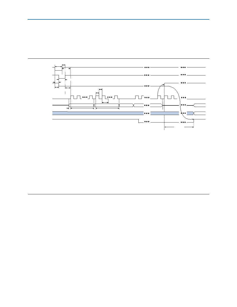
FPP Configuration Timing when DCLK to DATA[] > 1
Figure 21 shows the timing waveform for a FPP configuration when using a MAX II
device or microprocessor as an external host. This waveform shows timing when the
DCLK
-to-DATA[]ratio is more than 1.
Figure 21. FPP Configuration Timing Waveform When the DCLK-to-DATA[] Ratio is >1 (1)
Notes to Figure 21:
(1) The beginning of this waveform shows the device in user mode. In user mode, nCONFIG, nSTATUS, and CONF_DONE are at logic high levels.
When nCONFIG is pulled low, a reconfiguration cycle begins.
(2) After power up, the Arria V device holds nSTATUS low for the time as specified by the POR delay.
(3) After power up, before and during configuration, CONF_DONE is low.
(4) Do not leave DCLK floating after configuration. You can drive it high or low, whichever is more convenient.
(5) “r” denotes the DCLK-to-DATA[] ratio. For the DCLK-to-DATA[] ratio based on the decompression and the design security feature enable
settings, refer to Table 54 on page 1–52.
(6) If needed, pause DCLK by holding it low. When DCLK restarts, the external host must provide data on the DATA[15..0] pins prior to sending
the first DCLK rising edge.
(7) To ensure a successful configuration, send the entire configuration data to the Arria V device. CONF_DONE is released high after the Arria V device
receives all the configuration data successfully. After CONF_DONE goes high, send two additional falling edges on DCLK to begin initialization
and enter user mode.
(8) After the option bit to enable the INIT_DONE pin is configured into the device, the INIT_DONE goes low.
nCONFIG
nSTATUS (2)
CONF_DONE
(3)
DCLK (5)
DATA[15..0] (7)
User I/O
INIT_DONE
tCD2UM
tCF2ST1
tCF2CD
tCFG
tCF2CK
t
tCF2ST0
tST2CK
High-Z
User Mod
12
r
1
2
r
12
Word 0
Word 1
Word 3
1
tDSU
tDH
STATUS
tDH
tCH
tCL
tCLK
Word (n-1)
(6)
(7)
(8)
(4)
User Mod
r
相關(guān)PDF資料 |
PDF描述 |
|---|---|
| 5CGXFC7D7F31C8NES | IC CYCLONE V FPGA 150K 896-FBGA |
| 668-0003-C | IC CPU RABBIT2000 30MHZ 100PQFP |
| 668-0011 | IC MPU RABIT3000A 55.5MHZ128LQFP |
| 6PAIC3106IRGZRQ1 | IC AUDIO CODEC STEREO 48-QFN |
| 70001851 | DEVICE SERVER 1PORT SRL-ETHERNET |
相關(guān)代理商/技術(shù)參數(shù) |
參數(shù)描述 |
|---|---|
| 5AGXMB3G6F35C6N | 功能描述:FPGA - 現(xiàn)場可編程門陣列 FPGA - Arria V GX 13688 LABs 544 IOs RoHS:否 制造商:Altera Corporation 系列:Cyclone V E 柵極數(shù)量: 邏輯塊數(shù)量:943 內(nèi)嵌式塊RAM - EBR:1956 kbit 輸入/輸出端數(shù)量:128 最大工作頻率:800 MHz 工作電源電壓:1.1 V 最大工作溫度:+ 70 C 安裝風(fēng)格:SMD/SMT 封裝 / 箱體:FBGA-256 |
| 5AGXMB3G6F40C6N | 功能描述:FPGA - 現(xiàn)場可編程門陣列 FPGA - Arria V GX 13688 LABs 704 IOs RoHS:否 制造商:Altera Corporation 系列:Cyclone V E 柵極數(shù)量: 邏輯塊數(shù)量:943 內(nèi)嵌式塊RAM - EBR:1956 kbit 輸入/輸出端數(shù)量:128 最大工作頻率:800 MHz 工作電源電壓:1.1 V 最大工作溫度:+ 70 C 安裝風(fēng)格:SMD/SMT 封裝 / 箱體:FBGA-256 |
| 5AGXMB5G4F35C4N | 功能描述:FPGA - 現(xiàn)場可編程門陣列 FPGA - Arria V GX 15849 LABs 544 IOs RoHS:否 制造商:Altera Corporation 系列:Cyclone V E 柵極數(shù)量: 邏輯塊數(shù)量:943 內(nèi)嵌式塊RAM - EBR:1956 kbit 輸入/輸出端數(shù)量:128 最大工作頻率:800 MHz 工作電源電壓:1.1 V 最大工作溫度:+ 70 C 安裝風(fēng)格:SMD/SMT 封裝 / 箱體:FBGA-256 |
| 5AGXMB5G4F35C5G | 功能描述:1152-PIN FBGA 制造商:altera 系列:Arria V GX 零件狀態(tài):在售 LAB/CLB 數(shù):19811 邏輯元件/單元數(shù):420000 總 RAM 位數(shù):23625728 I/O 數(shù):544 電壓 - 電源:1.07 V ~ 1.13 V 工作溫度:0°C ~ 85°C(TJ) 標(biāo)準(zhǔn)包裝:24 |
| 5AGXMB5G4F35C5N | 功能描述:FPGA - 現(xiàn)場可編程門陣列 FPGA - Arria V GX 15849 LABs 544 IOs RoHS:否 制造商:Altera Corporation 系列:Cyclone V E 柵極數(shù)量: 邏輯塊數(shù)量:943 內(nèi)嵌式塊RAM - EBR:1956 kbit 輸入/輸出端數(shù)量:128 最大工作頻率:800 MHz 工作電源電壓:1.1 V 最大工作溫度:+ 70 C 安裝風(fēng)格:SMD/SMT 封裝 / 箱體:FBGA-256 |
發(fā)布緊急采購,3分鐘左右您將得到回復(fù)。