- 您現(xiàn)在的位置:買賣IC網(wǎng) > PDF目錄371612 > 55VDMOSFULL-BRIDGEMOTORDRIVER (647.67 k) PDF資料下載
參數(shù)資料
| 型號: | 55VDMOSFULL-BRIDGEMOTORDRIVER |
| 英文描述: | (647.67 k) |
| 中文描述: | (647.67十一) |
| 文件頁數(shù): | 8/18頁 |
| 文件大小: | 647K |
| 代理商: | 55VDMOSFULL-BRIDGEMOTORDRIVER |
Functional Descriptions
(Continued)
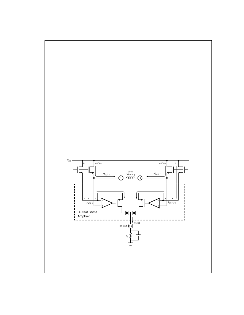
THE CURRENT SENSE AMPLIFIER
Many transistor cells in parallel make up the DMOS power
switches. The current sense amplifier (Figure 4 ) uses a
small fraction of the cells of both upper switches to provide a
unique, low-loss means for sensing the load current. In prac-
tice, each upper switch functions as a 1x sense device in
parallel with a 4000x power device. The current sense ampli-
fier forces the voltage at the source of the sense device to
equal that at the source of the power device; thus, the de-
vices share the total drain current in proportion to the 1:4000
cell ratio. Only the current flowing from drain to source, the
forward current, registers at the output of the current sense
amplifier. The current sense amplifier, therefore, sources
250 μA per ampere of total forward current conducted by the
upper two switches of the power bridge.
The sense current develops a potential across R
that is pro-
portional to the load current; for example, per ampere of load
current, the sense current develops one volt across a 4 k
resistor (the product of 250 μA per ampere and 4 k
). Since
chopping of the load current occurs as the voltage at CS
OUT surpasses the threshold (the DAC output voltage), R
S
sets the gain of the chopper amplifier; for example, a 2 k
resistor sets the gain at two amperes of load current per volt
of the threshold (the reciprocal of the product of 250 μA per
ampere and 2 k
). A quarter watt resistor suffices. A low
value capacitor connected in parallel with R
filters the ef-
fects of switching noise from the current sense signal.
While the specified maximum DC voltage compliance at CS
OUT is 12V, the specified operating voltage range at CS
OUT is 0V to 5V.
THE DIGITAL-TO-ANALOG CONVERTER (DAC)
The DAC sets the threshold voltage for chopping at
V
x D/16, where D is the decimal equivalent (0–15)
of the binary number applied at M4 through M1, the digital in-
puts of the DAC. M4 is the MSB or most significant bit. For
applications that require higher resolution, an external DAC
can drive the DAC REF input. While the specified maximum
DC voltage compliance at DAC REF is 12V, the specified op-
erating voltage range at DAC REF is 0V to 5V.
THE COMPARATOR, MONOSTABLE AND WINDING
CURRENT THRESHOLD FOR CHOPPING
As the voltage at CS OUT surpasses that at the output of the
DAC, the comparator triggers the monostable, and the
monostable, once triggered, provides a timing pulse to the
control logic. During the timing pulse, the power bridge
shorts the motor winding, causing current in the winding to
recirculate and decay slowly towards zero (Figure 1b and
Figure 1e again). A parallel resistor-capacitor network con-
nected between RC (pin
#
3) and ground sets the timing
pulse or off-time at about 1.1 RC seconds.
Chopping of the winding current occurs as the voltage at CS
OUT exceeds that at the output of the DAC; so chopping oc-
curs at a winding current threshold of about
(V
DAC REF
x D/16)
÷
((250 x 10
6
) x R
S
)) amperes.
DS011878-14
FIGURE 4. The Source Switches of the Power Bridge and the Current Sense Amplifier
www.national.com
8
相關(guān)PDF資料 |
PDF描述 |
|---|---|
| 56-G4009-032 | 56-G4009-032 |
| 56-G6005-001 | MARKETING OUTLINE - 16L CHIP SCALE BGA |
| 560-0303 | Optoelectronic |
| 560.425 | METER AIR VELOCITY T'SCOPIC PROBE |
| 5601053 | THERMOMETER MINI HANDHELD |
相關(guān)代理商/技術(shù)參數(shù) |
參數(shù)描述 |
|---|---|
| 5-5VFNHA2R | 制造商:Cooper Bussmann 功能描述:5.5KV USA RATED FUSE - Bulk |
| 5-5VFNHA3R | 制造商:Cooper Bussmann 功能描述:HV,MOTOR,USA,5500V,100A - Bulk |
| 5-5VFNHA4R | 制造商:Cooper Bussmann 功能描述:HV,MOTOR,USA,5500V,130A - Bulk |
| 5-5VFNHA6R | 制造商:Cooper Bussmann 功能描述:HV,MOTOR,USA,5500V,170A - Bulk |
| 5-5VKNHA12R | 制造商:Cooper Bussmann 功能描述:HV,MOTOR,USA,5500V,230A - Bulk |
發(fā)布緊急采購,3分鐘左右您將得到回復(fù)。