- 您現(xiàn)在的位置:買賣IC網(wǎng) > PDF目錄370100 > 2SJ605 (NEC Corp.) MOS FIELD EFFECT TRANSISTOR PDF資料下載
參數(shù)資料
| 型號(hào): | 2SJ605 |
| 廠商: | NEC Corp. |
| 英文描述: | MOS FIELD EFFECT TRANSISTOR |
| 中文描述: | MOS場效應(yīng)管 |
| 文件頁數(shù): | 2/8頁 |
| 文件大?。?/td> | 84K |
| 代理商: | 2SJ605 |
Data Sheet D14650EJ2V0DS
2
2SJ605
ELECTRICAL CHARACTERISTICS (T
A
= 25°C)
CHARACTERISTICS
SYMBOL
TEST CONDITIONS
MIN.
TYP.
MAX.
UNIT
Zero Gate Voltage Drain Current
I
DSS
V
DS
= –60
V, V
GS
= 0
V
–10
μ
A
Gate Leakage Current
I
GSS
V
GS
=
m
20
V, V
DS
= 0
V
m
10
μ
A
Gate Cut-off Voltage
V
GS(off)
V
DS
= –10
V, I
D
= –1
mA
–1.5
–2.0
–2.5
V
Forward Transfer Admittance
| y
fs
|
V
DS
= –10
V, I
D
= –33
A
30
59
S
Drain to Source On-state Resistance
R
DS(on)1
V
GS
= –10
V, I
D
= –33
A
17
20
m
R
DS(on)2
V
GS
= –4.0
V, I
D
= –33
A
22
31
m
Input Capacitance
C
iss
V
DS
= –10
V
4600
pF
Output Capacitance
C
oss
V
GS
= 0
V
820
pF
Reverse Transfer Capacitance
C
rss
f = 1
MHz
330
pF
Turn-on Delay Time
t
d(on)
V
DD
= –30
V, I
D
= –33
A
15
ns
Rise Time
t
r
V
GS
= –10
V
14
ns
Turn-off Delay Time
t
d(off)
R
G
= 0
100
ns
Fall Time
t
f
58
ns
Total Gate Charge
Q
G
V
DD
= –48
V
87
nC
Gate to Source Charge
Q
GS
V
GS
= –10
V
15
nC
Gate to Drain Charge
Q
GD
I
D
= –65
A
22
nC
Body Diode Forward Voltage
V
F(S-D)
I
F
= 65
A, V
GS
= 0
V
1.0
V
Reverse Recovery Time
t
rr
I
F
= 65
A, V
GS
= 0
V
53
ns
Reverse Recovery Charge
Q
rr
di/dt = 100
A
/
μ
s
110
nC
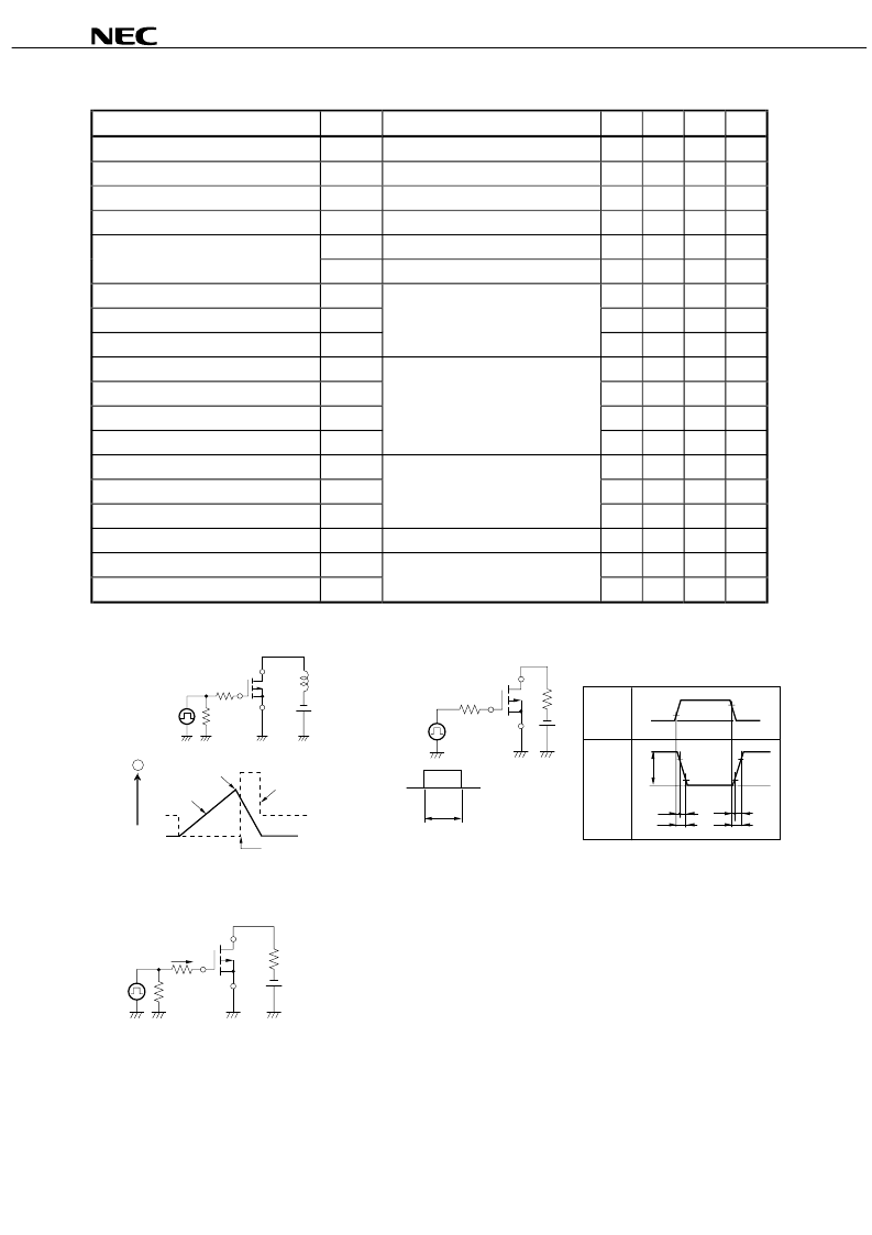
TEST CIRCUIT 1 AVALANCHE CAPABILITY
R
G
= 25
50
PG
L
V
DD
V
GS
= –20 V
→
0 V
BV
DSS
I
AS
I
D
V
DS
Starting T
ch
V
DD
D.U.T.
TEST CIRCUIT 3 GATE CHARGE
TEST CIRCUIT 2 SWITCHING TIME
PG.
R
G
0
V
GS
(
)
D.U.T.
R
L
V
DD
τ
= 1
s
Duty Cycle
≤
1%
μ
V
GS
Wave Form
V
DS
Wave Form
V
GS
(
)
10%
90%
10%
0
V
DS
(
)
90%
90%
t
d(on)
t
r
t
d(off)
t
f
10%
τ
V
DS
0
t
on
t
off
PG.
50
D.U.T.
R
L
V
DD
I
G
=
2 mA
!
!
!
!
!
!
相關(guān)PDF資料 |
PDF描述 |
|---|---|
| 2SJ605-S | MOS FIELD EFFECT TRANSISTOR |
| 2SJ605-Z | MOS FIELD EFFECT TRANSISTOR |
| 2SJ605-ZJ | MOS FIELD EFFECT TRANSISTOR |
| 2SJ606 | Box-shaped pin header, Discrete wire crimping connection, Discrete wire connectors; HRS No: 543-0712-0 00; No. of Positions: 32; Connector Type: Panel; Contact Gender: Male; Contact Spacing (mm): 2; Terminal Pitch (mm): 2; Current Rating(Amps)(Max.): 2; Contact Mating Area Plating: Tin; Operating Temperature Range (degrees C): -30 to 85; General Description: In-line adapter; Both ends male contacts; Pin contact |
| 2SJ606-S | Box-shaped pin header, Discrete wire crimping connection, Discrete wire connectors; HRS No: 543-0633-6 00; No. of Positions: 32; Connector Type: Panel; Contact Gender: Male; Contact Spacing (mm): 2; Terminal Pitch (mm): 2; Current Rating(Amps)(Max.): 2; Operating Temperature Range (degrees C): -30 to 85; General Description: In-line plug; Male contact; Pin contact termination |
相關(guān)代理商/技術(shù)參數(shù) |
參數(shù)描述 |
|---|---|
| 2SJ605-AZ | 制造商:Renesas Electronics Corporation 功能描述:Trans MOSFET P-CH 60V 65A 3-Pin(3+Tab) TO-220AB |
| 2SJ605-S | 制造商:NEC 制造商全稱:NEC 功能描述:MOS FIELD EFFECT TRANSISTOR |
| 2SJ605-Z | 制造商:NEC 制造商全稱:NEC 功能描述:MOS FIELD EFFECT TRANSISTOR |
| 2SJ605-Z-AZ | 制造商:Renesas Electronics Corporation 功能描述:Trans MOSFET P-CH 60V 65A 3-Pin(2+Tab) TO-220 SMD |
| 2SJ605-ZJ | 制造商:NEC 制造商全稱:NEC 功能描述:MOS FIELD EFFECT TRANSISTOR |
發(fā)布緊急采購,3分鐘左右您將得到回復(fù)。