- 您現(xiàn)在的位置:買賣IC網(wǎng) > PDF目錄370100 > 2SJ603 (NEC Corp.) MOS FIELD EFFECT TRANSISTOR PDF資料下載
參數(shù)資料
| 型號: | 2SJ603 |
| 廠商: | NEC Corp. |
| 英文描述: | MOS FIELD EFFECT TRANSISTOR |
| 中文描述: | MOS場效應(yīng)管 |
| 文件頁數(shù): | 7/8頁 |
| 文件大小: | 79K |
| 代理商: | 2SJ603 |
Data Sheet D14648EJ3V0DS
7
2SJ603
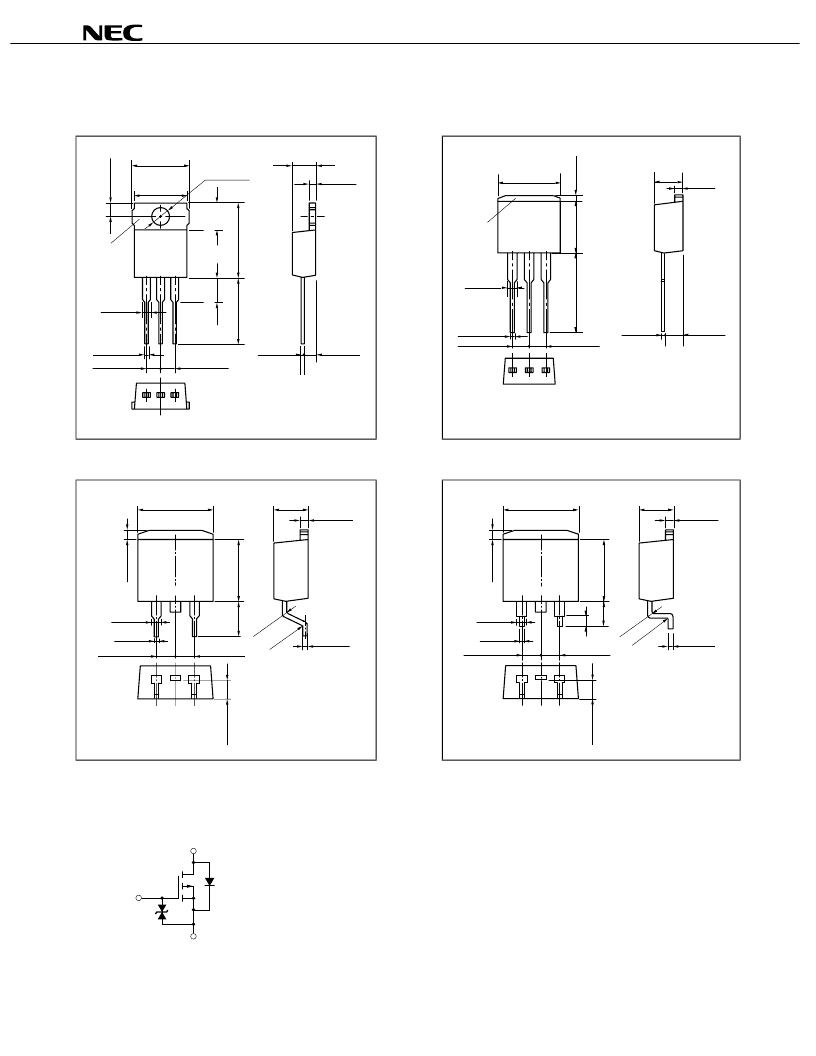
PACKAGE DRAWINGS (Unit: mm)
1)
TO-220AB (MP-25)
2)
TO-262 (MP-25 Fin Cut)
4.8 MAX.
1.Gate
2.Drain
3.Source
4.Fin (Drain)
1 2 3
10.6 MAX.
10.0 TYP.
3.6±0.2
φ
4
3
1.3±0.2
0.75±0.1
2.54 TYP.
2.54 TYP.
5
6
1
1
1.3±0.2
0.5±0.2
2.8±0.2
4.8 MAX.
1.Gate
2.Drain
3.Source
4.Fin (Drain)
1
2
3
10 TYP.
1.3±0.2
0.75±0.3
2.54 TYP.
2.54 TYP.
8
1
1.3±0.2
0.5±0.2
2.8±0.2
1
4
3)
TO-263 (MP-25ZJ)
4)
TO-220SMD (MP-25Z)
Note
1.4±0.2
1
2.54 TYP.
2.54 TYP.
8
1
2
3
5
4
4.8 MAX.
1.3±0.2
0.5±0.2
1.Gate
2.Drain
3.Source
4.Fin (Drain)
0.7±0.2
10 TYP.
05RTYP
08RTYP
2
10 TYP.
1.4±0.2
1
2.54 TYP.
2.54 TYP.
8
1
2
3
3
1
4
4.8 MAX.
1.3±0.2
0.5±0.2
05RTYP
08RTYP
0.75±0.3
2
1.Gate
2.Drain
3.Source
4.Fin (Drain)
Note
This package is produced only in Japan.
EQUIVALENT CIRCUIT
Source
Body
Diode
Gate
Protection
Diode
Gate
Drain
Remark
The diode connected between the gate and source of the transistor
serves as a protector against ESD. When this device actually used,
an additional protection circuit is externally required if a voltage
exceeding the rated voltage may be applied to this device.
#
相關(guān)PDF資料 |
PDF描述 |
|---|---|
| 2SJ603-S | MOS FIELD EFFECT TRANSISTOR |
| 2SJ603-Z | Box-shaped pin header, Discrete wire crimping connection, Discrete wire connectors; HRS No: 543-0514-7 00; No. of Positions: 30; Connector Type: Wire; Contact Gender: Female; Contact Spacing (mm): 2; Terminal Pitch (mm): 2; Current Rating(Amps)(Max.): 2; Operating Temperature Range (degrees C): -30 to 85; General Description: Housing; For Discrete wire; Crimping |
| 2SJ604 | MOS FIELD EFFECT TRANSISTOR |
| 2SJ604-S | MOS FIELD EFFECT TRANSISTOR |
| 2SJ604-Z | MOS FIELD EFFECT TRANSISTOR |
相關(guān)代理商/技術(shù)參數(shù) |
參數(shù)描述 |
|---|---|
| 2SJ603-S | 制造商:NEC 制造商全稱:NEC 功能描述:MOS FIELD EFFECT TRANSISTOR |
| 2SJ603-Z | 制造商:NEC 制造商全稱:NEC 功能描述:MOS FIELD EFFECT TRANSISTOR |
| 2SJ603-ZJ | 制造商:NEC 制造商全稱:NEC 功能描述:MOS FIELD EFFECT TRANSISTOR |
| 2SJ604 | 制造商:NEC 制造商全稱:NEC 功能描述:MOS FIELD EFFECT TRANSISTOR |
| 2SJ604-AZ | 制造商:Renesas Electronics 功能描述:Pch -60V -45A 30m@10V TO220AB Bulk 制造商:Renesas Electronics 功能描述:Pch -60V -45A 30m@10V TO220AB Cut Tape 制造商:Renesas Electronics Corporation 功能描述:Pch MOSFET,60V,45A,23m ohm,TO-220AB 制造商:Renesas 功能描述:Trans MOSFET P-CH 60V 45A 3-Pin(3+Tab) TO-220AB |
發(fā)布緊急采購,3分鐘左右您將得到回復(fù)。