- 您現(xiàn)在的位置:買賣IC網(wǎng) > PDF目錄370060 > 2SB1571HZ (NEC Corp.) TRANSISTOR | BJT | PNP | 30V V(BR)CEO | 5A I(C) | TO-243 PDF資料下載
參數(shù)資料
| 型號(hào): | 2SB1571HZ |
| 廠商: | NEC Corp. |
| 英文描述: | TRANSISTOR | BJT | PNP | 30V V(BR)CEO | 5A I(C) | TO-243 |
| 中文描述: | 晶體管|晶體管|進(jìn)步黨| 30V的五(巴西)總裁| 5A條一(c)|至243 |
| 文件頁數(shù): | 1/4頁 |
| 文件大?。?/td> | 41K |
| 代理商: | 2SB1571HZ |
2001
PNP SILICON EPITAXIAL TRANSISTOR
2SB1571
PNP SILICON EPITAXIAL TRANSISTOR
DATA SHEET
Document No.
Date Published
Printed in Japan
D15930EJ2V0DS00 (2nd edition)
December 2001 NS CP(K)
The information in this document is subject to change without notice. Before using this document, please
confirm that this is the latest version.
Not all devices/types available in every country. Please check with local NEC representative for
availability and additional information.
FEATURES
Low V
CE(sat)
: V
CE(sat)1
≤
0.35 V
Complementary to 2SD2402
ABSOLUTE MAXIMUM RATINGS (T
A
= 25°C)
Collector to Base Voltage
Collector to Emitter Voltage
Emitter to Base Voltage
Collector Current (DC)
Collector Current (pulse)
Note1
Base Current (DC)
Base Current (pulse)
Note1
Total Power Dissipation
Note2
Junction Temperature
Storage Temperature Range
Notes 1.
PW
≤
10 ms, Duty Cycle
≤
50%
2.
When mounted on ceramic substrate of 16 cm
2
x 0.7 mm
V
CBO
V
CEO
V
EBO
I
C(DC)
I
C(pulse)
I
B(DC)
I
B(pulse)
P
T
T
j
T
stg
50
30
6.0
5.0
8.0
0.2
0.4
2.0
150
V
V
V
A
A
A
A
W
°C
°C
–55 to + 150
ELECTRICAL CHARACTERISTICS (T
A
= 25°C)
CHARACTERISTICS
SYMBOL
TEST CONDITIONS
MIN.
TYP.
MAX.
UNIT
Collector Cut-off Current
I
CBO
V
CB
=
50 V, I
E
= 0
100
nA
Emitter Cut-off Current
DC Current Gain
Note
I
EBO
V
EB
=
6.0 V, I
C
= 0
100
nA
h
FE1
V
CE
=
1.0 V, I
C
=
1.0 A
80
h
FE2
V
CE
=
1.0 V, I
C
=
2.0 A
100
200
400
Base to Emitter Voltage
Note
Collector Saturation Voltage
Note
Collector Saturation Voltage
Note
Base Saturation Voltage
Note
V
BE
V
CE
=
1.0 V, I
C
=
0.1 A
0.6
0.665
0.7
V
V
CE(sat)1
I
C
=
3.0 A, I
B
=
0.15 A
0.17
0.35
V
V
CE(sat)2
I
C
=
5.0 A, I
B
=
0.25 A
0.28
0.55
V
V
BE(sat)
I
C
=
3.0 A, I
B
=
0.15 A
0.89
1.2
V
Gain Bandwidth Product
f
T
V
CE
=
10 V, I
E
= 0.5 A
150
MHz
Output Capacitance
C
ob
V
CB
=
10 V, I
E
= 0, f = 1.0 MHz
100
pF
Turn-on Time
t
on
I
C
=
2.0 A, V
CC
=
10 V,
265
ns
Storage Time
t
stg
R
L
= 5.0
, I
B1
=
I
B2
=
0.1 A,
350
ns
Fall Time
Note
Pulsed: PW
≤
350
μ
s, Duty Cycle
≤
2%
t
f
50
ns
h
FE
CLASSFICATION
Marking
HX
HY
HZ
h
FE2
100 to 200
160 to 320
200 to 400
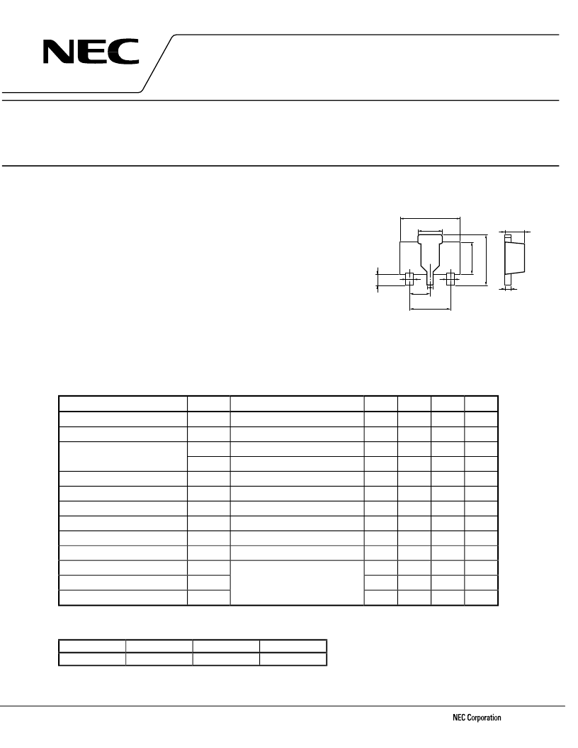
PACKAGE DRAWING (Unit: mm)
1.6±0.2
4.5±0.1
0.42
0
1.5
0.42
0.47
±0.06
3.0
2
4
0.41
+0.03
1.5±0.1
E
C
B
E: Emitter
C: Collector (Fin)
B: Base
相關(guān)PDF資料 |
PDF描述 |
|---|---|
| 2SB1587 | Silicon PNP Epitaxial Planar Transistor(Darlington)(硅PNP外延平面晶體管(達(dá)林頓)) |
| 2SB1588 | Silicon PNP Epitaxial Planar Transistor(Darlington)(硅PNP外延平面晶體管(達(dá)林頓)) |
| 2SB1590K | Power Transistor (-15V, -1A, 15V, 1A) |
| 2SD2444K | Power Transistor (-15V, -1A, 15V, 1A) |
| 2SB1616 | MEDIUM POWER TRANSISTER |
相關(guān)代理商/技術(shù)參數(shù) |
參數(shù)描述 |
|---|---|
| 2SB1571-T1-AZ(FY) | 制造商:Renesas Electronics 功能描述:PNP |
| 2SB1571-T1-AZ-FZ | 制造商:Renesas Electronics Corporation 功能描述: |
| 2SB1572-T1-AZ | 制造商:Renesas Electronics 功能描述:Cut Tape 制造商:Renesas Electronics Corporation 功能描述:PNP PWR Transistor,60V,3.0A,P-MINI MOLD3 制造商:Renesas 功能描述:Trans GP BJT PNP 60V 3A 4-Pin(3+Tab) SC-62 T/R |
| 2SB1572-T1-AZ HY | 制造商:Renesas Electronics 功能描述:PNP |
| 2SB1572-T1-AZ-HZ | 制造商:Renesas Electronics Corporation 功能描述: |
發(fā)布緊急采購,3分鐘左右您將得到回復(fù)。