- 您現(xiàn)在的位置:買賣IC網(wǎng) > PDF目錄371401 > 2501N (Fairchild Semiconductor Corporation) Dual N-Channel 2.5V Specified PowerTrench MOSFET PDF資料下載
參數(shù)資料
| 型號: | 2501N |
| 廠商: | Fairchild Semiconductor Corporation |
| 英文描述: | Dual N-Channel 2.5V Specified PowerTrench MOSFET |
| 中文描述: | 雙N溝道MOSFET的為2.5V指定的PowerTrench |
| 文件頁數(shù): | 2/5頁 |
| 文件大?。?/td> | 121K |
| 代理商: | 2501N |
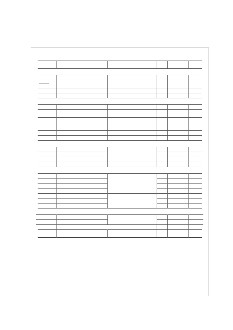
FDW2501N Rev E(W)
Electrical Characteristics
T
A
= 25°C unless otherwise noted
Test Conditions
Symbol
Parameter
Min
Typ Max Units
Off Characteristics
BV
DSS
BV
DSS
T
J
I
DSS
I
GSS
Drain–Source Breakdown Voltage
Breakdown Voltage Temperature
Coefficient
Zero Gate Voltage Drain Current
Gate–Body Leakage
V
GS
= 0 V,
I
D
= 250
μ
A
20
V
I
D
= 250
μ
A, Referenced to 25
°
C
12
mV/
°
C
V
DS
= 16 V,
V
GS
=
±
12 V,
V
GS
= 0 V
V
DS
= 0 V
1
μ
A
nA
±
100
On Characteristics
V
GS(th)
V
GS(th)
T
J
R
DS(on)
(Note 2)
Gate Threshold Voltage
Gate Threshold Voltage
Temperature Coefficient
Static Drain–Source
On–Resistance
V
DS
= V
GS
,
I
D
= 250
μ
A, Referenced to 25
°
C
I
D
= 250
μ
A
0.4
0.9
1.5
V
-3.2
mV/
°
C
V
GS
= 4.5 V,
V
GS
= 2.5 V,
V
GS
= 4.5 V, I
D
= 6.0A, T
J
=125
°
C
V
GS
= 4.5 V,
V
DS
= 5 V,
I
D
= 6.0 A
I
D
= 5.0 A
15.5
19.6
20
18
28
29
m
I
D(on)
g
FS
On–State Drain Current
Forward Transconductance
V
DS
= 5 V
I
D
= 6.0 A
30
A
S
32
Dynamic Characteristics
C
iss
Input Capacitance
C
oss
Output Capacitance
C
rss
Reverse Transfer Capacitance
R
G
Gate Resistance
1290
315
170
2.0
pF
pF
pF
V
DS
= 10 V,
f = 1.0 MHz
V
GS
= 0 V,
V
GS
= 15 mV,
f = 1.0 MHz
Switching Characteristics
t
d(on)
Turn–On Delay Time
t
r
Turn–On Rise Time
t
d(off)
Turn–Off Delay Time
t
f
Turn–Off Fall Time
Q
g
Total Gate Charge
Q
gs
Gate–Source Charge
Q
gd
Gate–Drain Charge
(Note 2)
10
15
26
9.5
12
2.4
3.3
18
27
47
19
17
ns
ns
ns
ns
nC
nC
nC
V
DD
= 10 V,
V
GS
= 4.5 V,
I
D
= 1 A,
R
GEN
= 6
V
DS
= 10 V,
V
GS
= 4.5 V
I
D
= 6.0 A,
Drain–Source Diode Characteristics and Maximum Ratings
t
rr
Diode Reverse Recovery Time
Q
rr
Diode Reverse Recovery Charge
I
S
Maximum Continuous Drain–Source Diode Forward Current
V
SD
Drain–Source Diode Forward
Voltage
20
6.7
nS
nC
I
F
= 6.0 A,
d
iF
/d
t
= 100 A/μs
0.83
1.2
A
V
V
GS
= 0 V,
I
S
= 0.83 A
(Note 2)
0.7
Notes:
1.
R
JA
is the sum of the junction-to-case and case-to-ambient thermal resistance where the case thermal reference is defined as the solder mounting surface of
the drain pins. R
θ
JC
is guaranteed by design while R
θ
CA
is determined by the user's board design.
a) R
θ
JA
is 125
°
C/W (steady state) when mounted on a 1 inch2 copper pad on FR-4.
b) R
θ
JA
is 208
°
C/W (steady state) when mounted on a minimum copper pad on FR-4.
2.
Pulse Test: Pulse Width < 300
μ
s, Duty Cycle < 2.0%
F
相關(guān)PDF資料 |
PDF描述 |
|---|---|
| 2502-2 | MOUNTING BRACKET KIT INSTALLATION INSTRUCTIONS |
| 2502P | Dual P-Channel 2.5V Specified PowerTrench MOSFET |
| 2507 | BUCHSE EINBAU DIN STANDARD 7POL |
| 25085 | KORROSIONSSPERRE 5L |
| 25093 | Low-Power, SPST, Fast, CMOS Analog Switch |
相關(guān)代理商/技術(shù)參數(shù) |
參數(shù)描述 |
|---|---|
| 2501NZ | 制造商:FAIRCHILD 制造商全稱:Fairchild Semiconductor 功能描述:Dual N-Channel 2.5V Specified PowerTrench MOSFET |
| 2501PDK40 | 制造商:n/a 功能描述:Diode Puck |
| 2501S1W34B | 制造商:SQUARE D 功能描述:Coil |
| 2501-W20-26-C3C | 制造商: 功能描述: 制造商:undefined 功能描述: |
| 250-1X | 制造商:TE Connectivity 功能描述: |
發(fā)布緊急采購,3分鐘左右您將得到回復(fù)。