- 您現(xiàn)在的位置:買賣IC網(wǎng) > PDF目錄382774 > ZR36055PQC21 PDF資料下載
參數(shù)資料
| 型號: | ZR36055PQC21 |
| 文件頁數(shù): | 5/16頁 |
| 文件大?。?/td> | 228K |
| 代理商: | ZR36055PQC21 |

ZR36011
5
PRELIMINARY
CONVERSION BYPASS
When the BYPASS control input is high, the color space conver-
sion block (Figure 1), and consequently the RGB <-> YCbCr
color space conversion computation, is bypassed. All the other
functional blocks, and all control inputs, continue to operate nor-
mally. Thus, when BYPASS is high, the device can be utilized as
a data format convertor, for example:
I
With CMY high, and MODE(2-0) = 000, as a RGB to CyMaYe
convertor
EF
235
111
-17
EE
235
110
-18
ED
235
109
-19
EC
235
108
-20
EB
235
107
-21
EA
234
106
-22
...
...
...
...
91
145
17
-111
90
144
16
-112
8F
143
15
-112
...
...
...
...
81
129
1
-112
80
128
0
-112
7F
127
-1
112
...
...
...
...
71
113
-15
112
70
112
-16
112
69
111
-17
111
...
...
...
...
11
17
-111
17
10
16
-112
16
0F
16
-112
15
...
...
...
01
16
-112
1
00
16
-112
0
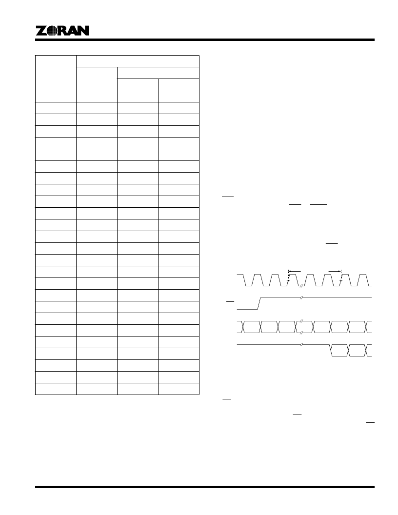
Table 3. Numerical Representation, CCIR = high (Continued)
Hexadecimal
Value
Decimal Equivalent
R, G, B, Y
(Unsigned)
CR, CB
Offset Binary
(SIGN = low)
Two’s
Compliment
(SIGN = high
I
With MODE(2-0) = 010, to perform conversions between
4:4:4 and 4:2:2 formats
With MODE(2-0) = 110, to perform 2:1 decimation and
interpolation of all three components
I
INPUT TO OUTPUT LATENCY
The output data has a latency or pipeline delay of eight clock
cycles. This latency is constant, in all modes of operation,
regardless of the direction of conversion, decimation or interpo-
lation setting, or whether the color space conversion is bypassed
or not.
DELAY LINE
The delay line consists of an eight stage shift register with a two
bit wide data path. Its delay is equal to the latency of the data
outputs. Thus, it is useful as a matching delay line for horizontal
and vertical video synchronization signals, to keep them in syn-
chronization with the data flowing through the device.
The RST input resets all stages of the delay line to the high state,
and consequently the output (SYC or SRGB depending on the
state of DIR) is also high when reset is active. The delay line is
therefore suitable for active low synchronization signals. The
input at SYC or SRGB is effectively ignored when RST is active,
and is clocked into the delay line starting from the second rising
edge of CLK following the deactivation of RST, as shown in
Figure 2.
OUTPUT ENABLE AND PIPELINE FREEZE
The OE input simultaneously controls the enabling of all output
pins (color components and delay line), and the freezing of the
computational pipeline. When OE is low, the output pins are
enabled, and data is clocked through the pipeline. When OE
goes high, the outputs go into a high impedance state, and the
clock is disabled internally starting at the second rising edge of
CLK following the rising edge of OE, thus freezing all operations
in their current state, including the color space conversion com-
putation, decimation and interpolation, and the delay line. Input
data is ignored while the clock is disabled. The clock is enabled
CLK
RST
Delay Line
Input
Data
(0)
Data
(7)
Data
(8)
Data
(9)
Delay Line
Output
Data
(0)
Data
(1)
8 Clock Cycles
Figure 2. Delay Line Reset Timing
相關(guān)PDF資料 |
PDF描述 |
|---|---|
| ZR36055PQC29.5 | |
| ZR36057PQC | |
| ZR36060PQC-27 | |
| ZR36060PQC-29.5 | |
| ZR36067PQC-LV | Peripheral IC |
相關(guān)代理商/技術(shù)參數(shù) |
參數(shù)描述 |
|---|---|
| ZR36055PQC29.5 | 制造商:未知廠家 制造商全稱:未知廠家 功能描述: |
| ZR36057 | 制造商:ZORAN 制造商全稱:ZORAN 功能描述:ENHANCED PCI BUS MULTIMEDIA CONTROLLER |
| ZR36057PQC | 制造商:ZORAN 制造商全稱:ZORAN 功能描述:ENHANCED PCI BUS MULTIMEDIA CONTROLLER |
| ZR36060 | 制造商:未知廠家 制造商全稱:未知廠家 功能描述:Integrated JPEG CODEC |
| ZR36060PQC | 制造商:未知廠家 制造商全稱:未知廠家 功能描述:Integrated JPEG CODEC |
發(fā)布緊急采購,3分鐘左右您將得到回復(fù)。