- 您現(xiàn)在的位置:買賣IC網(wǎng) > PDF目錄375045 > XQ2V6000-4FG456N (Xilinx, Inc.) QPro Virtex-II 1.5V Military QML Platform FPGAs PDF資料下載
參數(shù)資料
| 型號(hào): | XQ2V6000-4FG456N |
| 廠商: | Xilinx, Inc. |
| 英文描述: | QPro Virtex-II 1.5V Military QML Platform FPGAs |
| 中文描述: | QPro的Virtex - II 1.5V的軍事QML第平臺(tái)FPGA |
| 文件頁(yè)數(shù): | 74/128頁(yè) |
| 文件大小: | 2738K |
| 代理商: | XQ2V6000-4FG456N |
第1頁(yè)第2頁(yè)第3頁(yè)第4頁(yè)第5頁(yè)第6頁(yè)第7頁(yè)第8頁(yè)第9頁(yè)第10頁(yè)第11頁(yè)第12頁(yè)第13頁(yè)第14頁(yè)第15頁(yè)第16頁(yè)第17頁(yè)第18頁(yè)第19頁(yè)第20頁(yè)第21頁(yè)第22頁(yè)第23頁(yè)第24頁(yè)第25頁(yè)第26頁(yè)第27頁(yè)第28頁(yè)第29頁(yè)第30頁(yè)第31頁(yè)第32頁(yè)第33頁(yè)第34頁(yè)第35頁(yè)第36頁(yè)第37頁(yè)第38頁(yè)第39頁(yè)第40頁(yè)第41頁(yè)第42頁(yè)第43頁(yè)第44頁(yè)第45頁(yè)第46頁(yè)第47頁(yè)第48頁(yè)第49頁(yè)第50頁(yè)第51頁(yè)第52頁(yè)第53頁(yè)第54頁(yè)第55頁(yè)第56頁(yè)第57頁(yè)第58頁(yè)第59頁(yè)第60頁(yè)第61頁(yè)第62頁(yè)第63頁(yè)第64頁(yè)第65頁(yè)第66頁(yè)第67頁(yè)第68頁(yè)第69頁(yè)第70頁(yè)第71頁(yè)第72頁(yè)第73頁(yè)當(dāng)前第74頁(yè)第75頁(yè)第76頁(yè)第77頁(yè)第78頁(yè)第79頁(yè)第80頁(yè)第81頁(yè)第82頁(yè)第83頁(yè)第84頁(yè)第85頁(yè)第86頁(yè)第87頁(yè)第88頁(yè)第89頁(yè)第90頁(yè)第91頁(yè)第92頁(yè)第93頁(yè)第94頁(yè)第95頁(yè)第96頁(yè)第97頁(yè)第98頁(yè)第99頁(yè)第100頁(yè)第101頁(yè)第102頁(yè)第103頁(yè)第104頁(yè)第105頁(yè)第106頁(yè)第107頁(yè)第108頁(yè)第109頁(yè)第110頁(yè)第111頁(yè)第112頁(yè)第113頁(yè)第114頁(yè)第115頁(yè)第116頁(yè)第117頁(yè)第118頁(yè)第119頁(yè)第120頁(yè)第121頁(yè)第122頁(yè)第123頁(yè)第124頁(yè)第125頁(yè)第126頁(yè)第127頁(yè)第128頁(yè)
QPro Virtex-II 1.5V Military QML Platform FPGAs
74
www.xilinx.com
1-800-255-7778
DS122 (v1.1) January 7, 2004
Product Specification
R
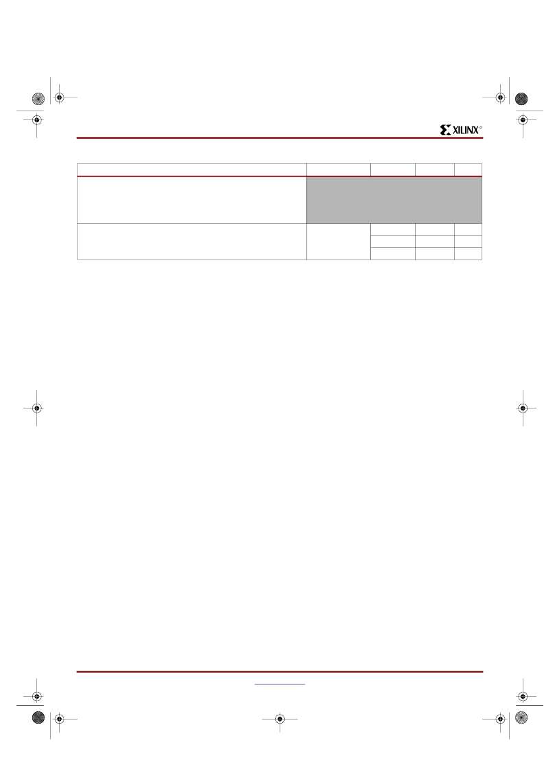
Table 71:
Pin-to-Pin Setup/Hold: Source-Synchronous Configuration
Description
Source Synchronous Timing Budgets
This section describes how to use the parameters provided
in the
Source-Synchronous Switching Characteristics
section to develop system-specific timing budgets. The fol-
lowing analysis provides information necessary for deter-
mining QPro Virtex-II contributions to an overall system
timing analysis. No assumptions are made about the effects
of Inter-Symbol Interference or PCB skew.
Symbol
Device
Value
Units
Data Input Set-Up and Hold Times Relative to a Forwarded Clock Input Pin,
Using DCM and Global Clock Buffer.
For situations where clock and data inputs conform to different standards,
adjust the setup and hold values accordingly using the values shown in
IOB
Input Switching Characteristics Standard Adjustments
, page 53
.
No Delay
Global Clock and IFF with DCM
T
PSDCM
/T
PHDCM
XQ2V1000
TBD
ns
XQ2V3000
TBD
ns
XQ2V6000
TBD
ns
Notes:
1.
2.
3.
IFF = Input Flip-Flop
The timing values were measured using the fine-phase adjustment feature of the DCM.
The worst-case duty-cycle distortion and DCM jitter on CLK0 and CLK180 is included in these measurements.
QPro Virtex-II Transmitter Data-Valid Window (T
X
)
T
X
is the minimum aggregate valid data period for a
source-synchronous data bus at the pins of the device and
is calculated as follows:
T
X
= Data Period - [Jitter
(1)
+ Duty Cycle Distortion
(2)
+
TCKSKEW
(3)
+ TPKGSKEW
(4)
]
Notes:
1.
Jitter values and accumulation methodology to be provided in
a future release of this document. The absolute period jitter
values found in the
DCM Timing Parameters
section of the
particular DCM output clock used to clock the IOB FF can be
used for a best-case analysis.
This value depends on the clocking methodology used. See
Note 1 for
Table 68
.
This value represents the worst-case clock-tree skew
observable between sequential I/O elements. Significantly
less clock-tree skew exists for I/O registers that are close to
each other and fed by the same or adjacent clock-tree
branches. Use the Xilinx FPGA_Editor and Timing Analyzer
tools to evaluate clock skew specific to your application.
These values represent the worst-case skew between any
two balls of the package: shortest flight time to longest flight
time from Pad to Ball.
2.
3.
4.
QPro Virtex-II Receiver Data-Valid Window (R
X
)
R
X
is the required minimum aggregate valid data period for
a source-synchronous data bus at the pins of the device
and is calculated as follows:
R
X
= [TSAMP
(1)
+ TCKSKEW
(2)
+ TPKGSKEW
(3)
]
Notes:
1.
This parameter indicates the total sampling error of QPro
Virtex-II
DDR input registers across voltage, temperature,
and process. The characterization methodology uses the
DCM to capture the DDR input registers’ edges of operation.
These measurements include:
-
CLK0 and CLK180 DCM jitter in a quiet system
-
Worst-case duty-cycle distortion
-
DCM accuracy (phase offset)
-
DCM phase shift resolution
These measurements do not include package or clock tree
skew.
2.
This value represents the worst-case clock-tree skew
observable between sequential I/O elements. Significantly
less clock-tree skew exists for I/O registers that are close to
each other and fed by the same or adjacent clock-tree
branches. Use the Xilinx FPGA_Editor and Timing Analyzer
tools to evaluate clock skew specific to your application.
3.
These values represent the worst-case skew between any
two balls of the package: shortest flight time to longest flight
time from Pad to Ball.
ds122_1_1.fm Page 74 Wednesday, January 7, 2004 9:15 PM
相關(guān)PDF資料 |
PDF描述 |
|---|---|
| XQ4005EX-4CB191N | QML High-Reliability FPGAs |
| XQ4005EX-3CB191M | QML High-Reliability FPGAs |
| XQ4005EX-3CB191N | QML High-Reliability FPGAs |
| XQ4005EX-3CB196M | QML High-Reliability FPGAs |
| XQ4005EX-3CB196N | QML High-Reliability FPGAs |
相關(guān)代理商/技術(shù)參數(shù) |
參數(shù)描述 |
|---|---|
| XQ2V6000-5EF1152I | 制造商:XILINX 制造商全稱:XILINX 功能描述:QPro Virtex-II 1.5V Platform FPGAs |
| XQ2V6000-5EF957I | 制造商:XILINX 制造商全稱:XILINX 功能描述:QPro Virtex-II 1.5V Platform FPGAs |
| XQ2V6000-BG575I | 制造商:XILINX 制造商全稱:XILINX 功能描述:QPro Virtex-II 1.5V Platform FPGAs |
| XQ2V6000-BG575M | 制造商:XILINX 制造商全稱:XILINX 功能描述:QPro Virtex-II 1.5V Platform FPGAs |
| XQ2V6000-BG575N | 制造商:XILINX 制造商全稱:XILINX 功能描述:QPro Virtex-II 1.5V Platform FPGAs |
發(fā)布緊急采購(gòu),3分鐘左右您將得到回復(fù)。