- 您現(xiàn)在的位置:買賣IC網(wǎng) > PDF目錄4272 > XCV50E-6FG256C (Xilinx Inc)IC FPGA 1.8V C-TEMP 256-FBGA PDF資料下載
參數(shù)資料
| 型號: | XCV50E-6FG256C |
| 廠商: | Xilinx Inc |
| 文件頁數(shù): | 167/233頁 |
| 文件大小: | 0K |
| 描述: | IC FPGA 1.8V C-TEMP 256-FBGA |
| 產(chǎn)品變化通告: | FPGA Family Discontinuation 18/Apr/2011 |
| 標準包裝: | 90 |
| 系列: | Virtex®-E |
| LAB/CLB數(shù): | 384 |
| 邏輯元件/單元數(shù): | 1728 |
| RAM 位總計: | 65536 |
| 輸入/輸出數(shù): | 176 |
| 門數(shù): | 71693 |
| 電源電壓: | 1.71 V ~ 1.89 V |
| 安裝類型: | 表面貼裝 |
| 工作溫度: | 0°C ~ 85°C |
| 封裝/外殼: | 256-BGA |
| 供應商設(shè)備封裝: | 256-FBGA(17x17) |
第1頁第2頁第3頁第4頁第5頁第6頁第7頁第8頁第9頁第10頁第11頁第12頁第13頁第14頁第15頁第16頁第17頁第18頁第19頁第20頁第21頁第22頁第23頁第24頁第25頁第26頁第27頁第28頁第29頁第30頁第31頁第32頁第33頁第34頁第35頁第36頁第37頁第38頁第39頁第40頁第41頁第42頁第43頁第44頁第45頁第46頁第47頁第48頁第49頁第50頁第51頁第52頁第53頁第54頁第55頁第56頁第57頁第58頁第59頁第60頁第61頁第62頁第63頁第64頁第65頁第66頁第67頁第68頁第69頁第70頁第71頁第72頁第73頁第74頁第75頁第76頁第77頁第78頁第79頁第80頁第81頁第82頁第83頁第84頁第85頁第86頁第87頁第88頁第89頁第90頁第91頁第92頁第93頁第94頁第95頁第96頁第97頁第98頁第99頁第100頁第101頁第102頁第103頁第104頁第105頁第106頁第107頁第108頁第109頁第110頁第111頁第112頁第113頁第114頁第115頁第116頁第117頁第118頁第119頁第120頁第121頁第122頁第123頁第124頁第125頁第126頁第127頁第128頁第129頁第130頁第131頁第132頁第133頁第134頁第135頁第136頁第137頁第138頁第139頁第140頁第141頁第142頁第143頁第144頁第145頁第146頁第147頁第148頁第149頁第150頁第151頁第152頁第153頁第154頁第155頁第156頁第157頁第158頁第159頁第160頁第161頁第162頁第163頁第164頁第165頁第166頁當前第167頁第168頁第169頁第170頁第171頁第172頁第173頁第174頁第175頁第176頁第177頁第178頁第179頁第180頁第181頁第182頁第183頁第184頁第185頁第186頁第187頁第188頁第189頁第190頁第191頁第192頁第193頁第194頁第195頁第196頁第197頁第198頁第199頁第200頁第201頁第202頁第203頁第204頁第205頁第206頁第207頁第208頁第209頁第210頁第211頁第212頁第213頁第214頁第215頁第216頁第217頁第218頁第219頁第220頁第221頁第222頁第223頁第224頁第225頁第226頁第227頁第228頁第229頁第230頁第231頁第232頁第233頁
Virtex-E 1.8 V Field Programmable Gate Arrays
R
DS022-2 (v3.0) March 21, 2014
Module 2 of 4
Production Product Specification
33
— OBSOLETE — OBSOLETE — OBSOLETE — OBSOLETE —
standard requires a Differential Amplifier input buffer and a
Push-Pull output buffer.
SSTL3 — Stub Series Terminated Logic for 3.3V
The Stub Series Terminated Logic for 3.3V, or SSTL3 stan-
dard is a general purpose 3.3V memory bus standard also
sponsored by Hitachi and IBM (JESD8-8). This standard
has two classes, I and II. SelectI/O devices support both
classes for the SSTL3 standard. This standard requires a
Differential Amplifier input buffer and an Push-Pull output
buffer.
SSTL2 — Stub Series Terminated Logic for 2.5V
The Stub Series Terminated Logic for 2.5V, or SSTL2 stan-
dard is a general purpose 2.5V memory bus standard spon-
sored by Hitachi and IBM (JESD8-9). This standard has two
classes, I and II. SelectI/O devices support both classes for
the SSTL2 standard. This standard requires a Differential
Amplifier input buffer and an Push-Pull output buffer.
CTT — Center Tap Terminated
The Center Tap Terminated, or CTT standard is a 3.3V
memory bus standard sponsored by Fujitsu (JESD8-4).
This standard requires a Differential Amplifier input buffer
and a Push-Pull output buffer.
AGP-2X — Advanced Graphics Port
The Intel AGP standard is a 3.3V Advanced Graphics
Port-2X bus standard used with the Pentium II processor for
graphics applications. This standard requires a Push-Pull
output buffer and a Differential Amplifier input buffer.
LVDS — Low Voltage Differential Signal
LVDS is a differential I/O standard. It requires that one data
bit is carried through two signal lines. As with all differential
signaling standards, LVDS has an inherent noise immunity
over single-ended I/O standards. The voltage swing
between two signal lines is approximately 350mV. The use
of a reference voltage (VREF) or a board termination voltage
(VTT) is not required. LVDS requires the use of two pins per
input or output. LVDS requires external resistor termination.
BLVDS — Bus LVDS
This standard allows for bidirectional LVDS communication
between two or more devices. The external resistor termi-
nation is different than the one for standard LVDS.
LVPECL — Low Voltage Positive Emitter Coupled
Logic
LVPECL is another differential I/O standard. It requires two
signal lines for transmitting one data bit. This standard
specifies two pins per input or output. The voltage swing
between these two signal lines is approximately 850 mV.
The use of a reference voltage (VREF) or a board termina-
tion voltage (VTT) is not required. The LVPECL standard
requires external resistor termination.
Library Symbols
The Xilinx library includes an extensive list of symbols
designed to provide support for the variety of SelectI/O fea-
tures. Most of these symbols represent variations of the five
generic SelectI/O symbols.
IBUF (input buffer)
IBUFG (global clock input buffer)
OBUF (output buffer)
OBUFT (3-state output buffer)
IOBUF (input/output buffer)
IBUF
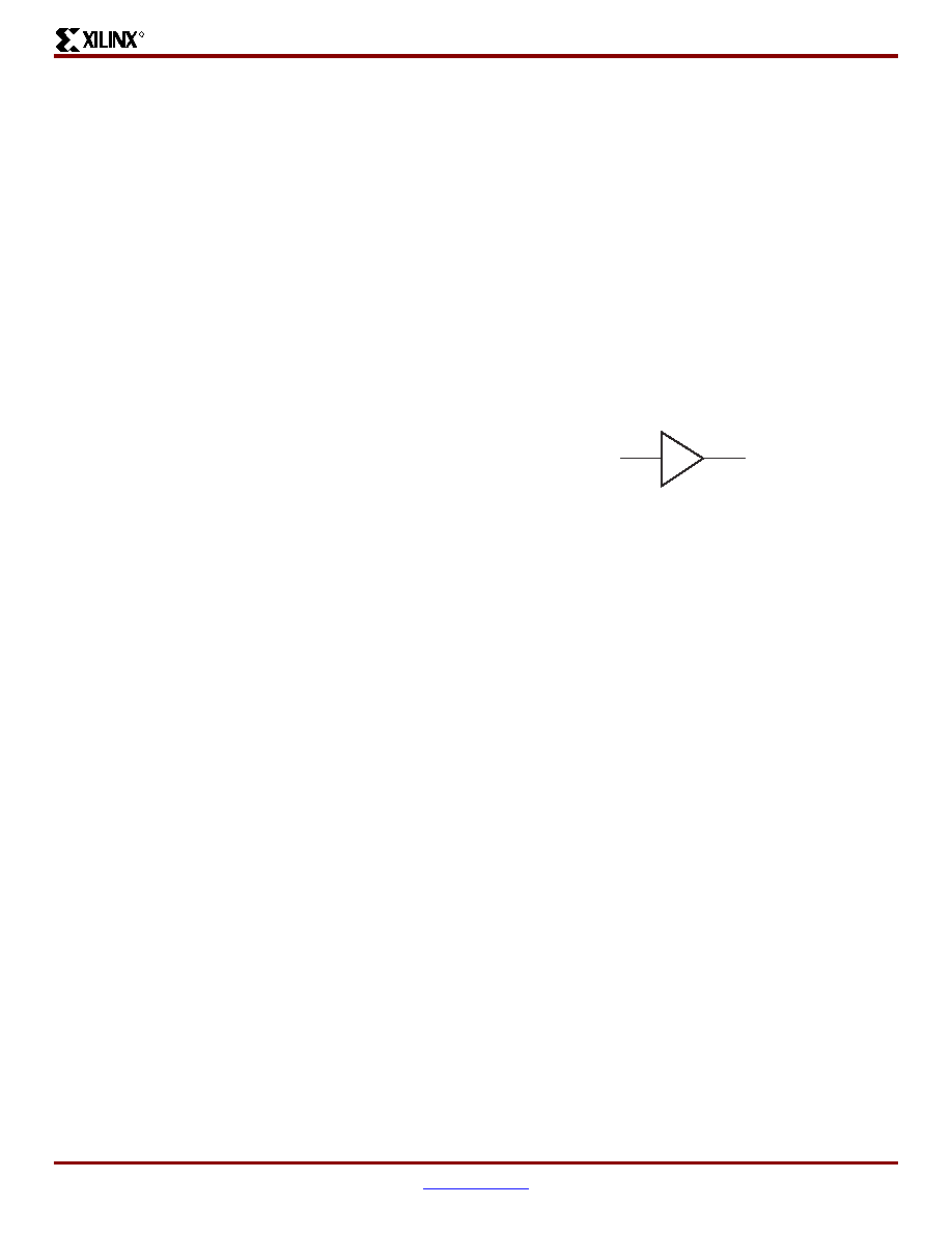
Signals used as inputs to the Virtex-E device must source
an input buffer (IBUF) via an external input port. The generic
Virtex-E IBUF symbol appears in Figure 37. The extension
to the base name defines which I/O standard the IBUF
uses. The assumed standard is LVTTL when the generic
IBUF has no specified extension.
The following list details the variations of the IBUF symbol:
IBUF
IBUF_LVCMOS2
IBUF_PCI33_3
IBUF_PCI66_3
IBUF_GTL
IBUF_GTLP
IBUF_HSTL_I
IBUF_HSTL_III
IBUF_HSTL_IV
IBUF_SSTL3_I
IBUF_SSTL3_II
IBUF_SSTL2_I
IBUF_SSTL2_II
IBUF_CTT
IBUF_AGP
IBUF_LVCMOS18
IBUF_LVDS
IBUF_LVPECL
When the IBUF symbol supports an I/O standard that
requires a VREF, the IBUF automatically configures as a dif-
ferential amplifier input buffer. The VREF voltage must be
supplied on the VREF pins. In the case of LVDS, LVPECL,
and BLVDS, VREF is not required.
Figure 37: Input Buffer (IBUF) Symbols
O
I
IBUF
x133_01_111699
相關(guān)PDF資料 |
PDF描述 |
|---|---|
| XC6SLX25-L1CSG324I | IC FPGA SPARTAN 6 24K 324CSGBGA |
| XC6SLX25-N3FGG484I | IC FPGA SPARTAN-6 484FBGA |
| HMC49DRXS-S734 | CONN EDGECARD 98POS DIP .100 SLD |
| XC6SLX25-2FG484I | IC FPGA SPARTAN 6 484FGGBGA |
| ACC49DRYN-S734 | CONN EDGECARD 98POS DIP .100 SLD |
相關(guān)代理商/技術(shù)參數(shù) |
參數(shù)描述 |
|---|---|
| XCV50E-6FG256C0773 | 制造商:Xilinx 功能描述: |
| XCV50E-6FG256I | 功能描述:IC FPGA 1.8V I-TEMP 256-FBGA RoHS:否 類別:集成電路 (IC) >> 嵌入式 - FPGA(現(xiàn)場可編程門陣列) 系列:Virtex®-E 標準包裝:40 系列:Spartan® 6 LX LAB/CLB數(shù):3411 邏輯元件/單元數(shù):43661 RAM 位總計:2138112 輸入/輸出數(shù):358 門數(shù):- 電源電壓:1.14 V ~ 1.26 V 安裝類型:表面貼裝 工作溫度:-40°C ~ 100°C 封裝/外殼:676-BGA 供應商設(shè)備封裝:676-FBGA(27x27) |
| XCV50E-6HQ240C | 制造商:XILINX 制造商全稱:XILINX 功能描述:Virtex⑩-E 1.8 V Field Programmable Gate Arrays |
| XCV50E-6HQ240I | 制造商:XILINX 制造商全稱:XILINX 功能描述:Virtex⑩-E 1.8 V Field Programmable Gate Arrays |
| XCV50E-6PQ240C | 功能描述:IC FPGA 1.8V C-TEMP 240-PQFP RoHS:否 類別:集成電路 (IC) >> 嵌入式 - FPGA(現(xiàn)場可編程門陣列) 系列:Virtex®-E 標準包裝:40 系列:Spartan® 6 LX LAB/CLB數(shù):3411 邏輯元件/單元數(shù):43661 RAM 位總計:2138112 輸入/輸出數(shù):358 門數(shù):- 電源電壓:1.14 V ~ 1.26 V 安裝類型:表面貼裝 工作溫度:-40°C ~ 100°C 封裝/外殼:676-BGA 供應商設(shè)備封裝:676-FBGA(27x27) |
發(fā)布緊急采購,3分鐘左右您將得到回復。