- 您現(xiàn)在的位置:買賣IC網(wǎng) > PDF目錄4173 > XCS40XL-4PQ240C (Xilinx Inc)IC 3.3V FPGA COMM. TEMP 240PQFP PDF資料下載
參數(shù)資料
| 型號(hào): | XCS40XL-4PQ240C |
| 廠商: | Xilinx Inc |
| 文件頁(yè)數(shù): | 5/83頁(yè) |
| 文件大?。?/td> | 0K |
| 描述: | IC 3.3V FPGA COMM. TEMP 240PQFP |
| 產(chǎn)品變化通告: | Product Discontinuation 26/Oct/2011 |
| 標(biāo)準(zhǔn)包裝: | 24 |
| 系列: | Spartan®-XL |
| LAB/CLB數(shù): | 784 |
| 邏輯元件/單元數(shù): | 1862 |
| RAM 位總計(jì): | 25088 |
| 輸入/輸出數(shù): | 192 |
| 門數(shù): | 40000 |
| 電源電壓: | 3 V ~ 3.6 V |
| 安裝類型: | 表面貼裝 |
| 工作溫度: | 0°C ~ 85°C |
| 封裝/外殼: | 240-BFQFP |
| 供應(yīng)商設(shè)備封裝: | 240-PQFP(32x32) |
| 其它名稱: | Q1039179A Q1150517 XCS40XL4PQ240C |
第1頁(yè)第2頁(yè)第3頁(yè)第4頁(yè)當(dāng)前第5頁(yè)第6頁(yè)第7頁(yè)第8頁(yè)第9頁(yè)第10頁(yè)第11頁(yè)第12頁(yè)第13頁(yè)第14頁(yè)第15頁(yè)第16頁(yè)第17頁(yè)第18頁(yè)第19頁(yè)第20頁(yè)第21頁(yè)第22頁(yè)第23頁(yè)第24頁(yè)第25頁(yè)第26頁(yè)第27頁(yè)第28頁(yè)第29頁(yè)第30頁(yè)第31頁(yè)第32頁(yè)第33頁(yè)第34頁(yè)第35頁(yè)第36頁(yè)第37頁(yè)第38頁(yè)第39頁(yè)第40頁(yè)第41頁(yè)第42頁(yè)第43頁(yè)第44頁(yè)第45頁(yè)第46頁(yè)第47頁(yè)第48頁(yè)第49頁(yè)第50頁(yè)第51頁(yè)第52頁(yè)第53頁(yè)第54頁(yè)第55頁(yè)第56頁(yè)第57頁(yè)第58頁(yè)第59頁(yè)第60頁(yè)第61頁(yè)第62頁(yè)第63頁(yè)第64頁(yè)第65頁(yè)第66頁(yè)第67頁(yè)第68頁(yè)第69頁(yè)第70頁(yè)第71頁(yè)第72頁(yè)第73頁(yè)第74頁(yè)第75頁(yè)第76頁(yè)第77頁(yè)第78頁(yè)第79頁(yè)第80頁(yè)第81頁(yè)第82頁(yè)第83頁(yè)
Spartan and Spartan-XL FPGA Families Data Sheet
DS060 (v2.0) March 1, 2013
13
Product Specification
R
Product Obsolete/Under Obsolescence
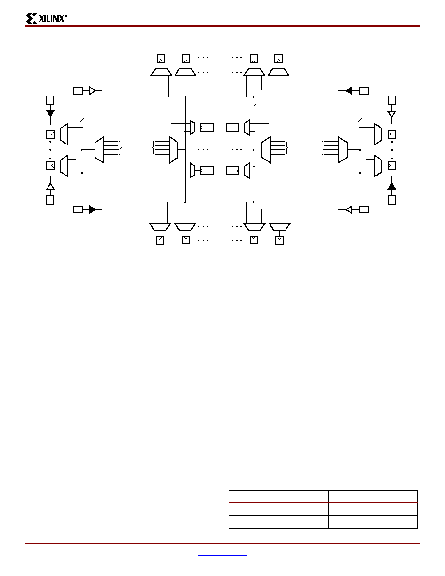
The four Primary Global buffers offer the shortest delay and
negligible skew. Four Secondary Global buffers have
slightly longer delay and slightly more skew due to poten-
tially heavier loading, but offer greater flexibility when used
to drive non-clock CLB inputs. The eight Global Low-Skew
buffers in the Spartan-XL devices combine short delay, neg-
ligible skew, and flexibility.
The Primary Global buffers must be driven by the semi-ded-
icated pads (PGCK1-4). The Secondary Global buffers can
be sourced by either semi-dedicated pads (SGCK1-4) or
internal nets. Each corner of the device has one Primary
buffer and one Secondary buffer. The Spartan-XL family
has eight global low-skew buffers, two in each corner. All
can be sourced by either semi-dedicated pads (GCK1-8) or
internal nets.
Using the library symbol called BUFG results in the software
choosing the appropriate clock buffer, based on the timing
requirements of the design. A global buffer should be spec-
ified for all timing-sensitive global signal distribution. To use
a global buffer, place a BUFGP (primary buffer), BUFGS
(secondary buffer), BUFGLS (Spartan-XL family global
low-skew buffer), or BUFG (any buffer type) element in a
schematic or in HDL code.
Advanced Features Description
Distributed RAM
Optional modes for each CLB allow the function generators
(F-LUT and G-LUT) to be used as Random Access Memory
(RAM).
Read and write operations are significantly faster for this
on-chip RAM than for off-chip implementations. This speed
advantage is due to the relatively short signal propagation
delays within the FPGA.
Memory Configuration Overview
There are two available memory configuration modes: sin-
gle-port RAM and dual-port RAM. For both these modes,
write operations are synchronous (edge-triggered), while
read operations are asynchronous. In the single-port mode,
a single CLB can be configured as either a 16 x 1, (16 x 1)
x 2, or 32 x 1 RAM array. In the dual-port mode, a single
CLB can be configured only as one 16 x 1 RAM array. The
different CLB memory configurations are summarized in
Table 8. Any of these possibilities can be individually pro-
grammed into a Spartan/XL FPGA CLB.
Figure 11: 5V Spartan Family Global Net Distribution
X4
ds060_11_080400
X4
4
One BUFGP
per Global Line
One BUFGP
per Global Line
Any BUFGS
BUFGP
PGCK4
SGCK4
PGCK3
SGCK3
BUFGS
BUFGP
BUFGS
IOB
BUFGS
BUFGP
SGCK1
PGCK1
SGCK2
PGCK2
IOB
X4
locals
4
CLB
locals
CLB
locals
Table 8: CLB Memory Configurations
Mode
16 x 1
(16 x 1) x 2
32 x 1
Single-Port
√√
√
Dual-Port
√
相關(guān)PDF資料 |
PDF描述 |
|---|---|
| IDT71V424L12YG8 | IC SRAM 4MBIT 12NS 36SOJ |
| IDT71V424L10YG8 | IC SRAM 4MBIT 10NS 36SOJ |
| IDT71V416L15YG8 | IC SRAM 4MBIT 15NS 44SOJ |
| IDT71V416L12YG8 | IC SRAM 4MBIT 12NS 44SOJ |
| IDT71V424S10PHGI8 | IC SRAM 4MBIT 10NS 44TSOP |
相關(guān)代理商/技術(shù)參數(shù) |
參數(shù)描述 |
|---|---|
| XCS40XL-4PQ240I | 制造商:XILINX 制造商全稱:XILINX 功能描述:Spartan and Spartan-XL Families Field Programmable Gate Arrays |
| XCS40XL-4PQ256C | 制造商:XILINX 制造商全稱:XILINX 功能描述:Spartan and Spartan-XL Families Field Programmable Gate Arrays |
| XCS40XL-4PQ256I | 制造商:XILINX 制造商全稱:XILINX 功能描述:Spartan and Spartan-XL Families Field Programmable Gate Arrays |
| XCS40XL-4PQ280C | 制造商:XILINX 制造商全稱:XILINX 功能描述:Spartan and Spartan-XL Families Field Programmable Gate Arrays |
| XCS40XL-4PQ280I | 制造商:XILINX 制造商全稱:XILINX 功能描述:Spartan and Spartan-XL Families Field Programmable Gate Arrays |
發(fā)布緊急采購(gòu),3分鐘左右您將得到回復(fù)。