- 您現(xiàn)在的位置:買賣IC網(wǎng) > PDF目錄372879 > XC9801BXX3DR (TOREX SEMICONDUCTOR LTD.) Step-Up Charge Pump ICs PDF資料下載
參數(shù)資料
| 型號: | XC9801BXX3DR |
| 廠商: | TOREX SEMICONDUCTOR LTD. |
| 英文描述: | Step-Up Charge Pump ICs |
| 中文描述: | 升壓充電泵集成電路 |
| 文件頁數(shù): | 2/10頁 |
| 文件大小: | 103K |
| 代理商: | XC9801BXX3DR |
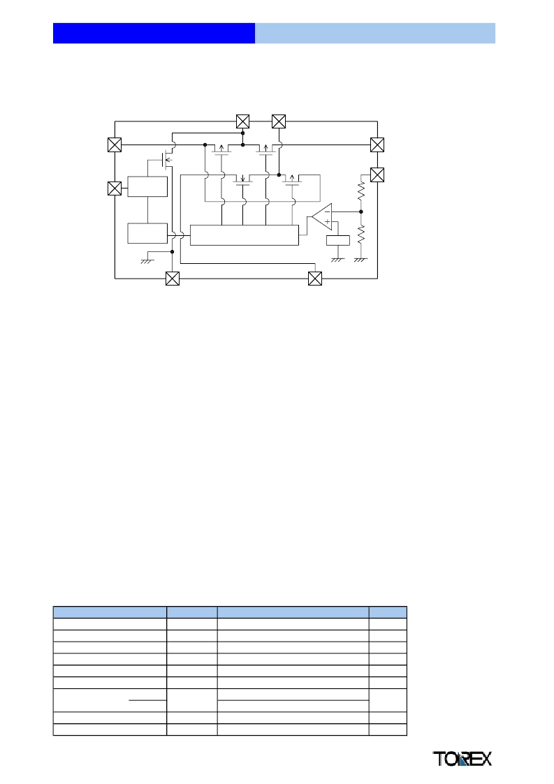
Block Diagram
(1) Basic Operations
Using the XC9801/02’s clock generated by the internal oscillator, a step-up charge pump operation can be brought
about as a result of the alternate switching between operating conditions where P1 & N4 are ON with P2 & P3 OFF
(or) P1 & N4 are OFF with P2 & P3 ON. By connecting the SENSE pin to VOUT, output voltage can be fedback and
the difference between the feedback voltage and the reference voltage (Vref) are compared by the internal operational
amplifier. Output voltage can be stabilized (Note 2) by controlling P3’s gate voltage waveform via the signal generated
by the internal amplifier.
Please note that this stabilizing function will not operate with VIN < (VOUT/2) or VIN
≥
VOUT.
By connecting SENSE to ground, the output stability function, as described above, can be halted and the IC can be
used as a step-up doubler.
(2) Stand-by Function
When the voltage at CE (chip enable) is ‘low’ (0V), P1,P2 & P3 will be OFF with N4 & N5 ON. The external capacitor
C1 will discharge and impedance at Vout will be high.
(3) PFM (Pulse Skip) Operations
Whilst maintaining output voltage, the XC9802 provides the added security of protection against drops in efficiency
during light loads as a result of the pulse, generated by the internal oscillator, being skipped and the operating
frequency being changed.
Absolute Maximum Ratings
Ta = 25
O
C, GND = 0V
CONDITIONS
-0.3
~
6
-0.3
~
12
-0.3
~
VOUT + 0.3
-0.3
~
VOUT + 0.3
-0.3
~
VIN + 0.3
200
150
MSOP-8A
USP-8
2
TBD
mW
Power dissipation
Pd
Note 2
: As a result of P3 gradually reaching an ON state with each clock (signal), rush current is controlled, the ripple
decreases and with the combination of the independent phase compensation circuit, output voltage is stabilized
- 40
~
+ 85
- 40
~
+ 125
UNITS
V
V
V
V
V
mA
V
CE
I
OUT
Operating Temperature
Storage Temperature
Topr
Tstg
O
C
O
C
C1 - pin voltage
CE pin voltage
V
OUT
pin output current
PARAMETER
V
IN
pin voltage
V
OUT
pin voltage
C1 + pin voltage
XC9801/02 Series
Step-Up Charge Pump ICs
SYMBOL
V
IN
V
OUT
C1+
C1-
VIN
CE
C1+
C1-
VOUT
SENSE
GND
PGND
Chip
Enable
Oscillator
Vref
Controler
P1
P2
P3
N4
N5
相關(guān)PDF資料 |
PDF描述 |
|---|---|
| XC9801BXX3KL | Step-Up Charge Pump ICs |
| XC9801BXX3KR | Step-Up Charge Pump ICs |
| XC9801 | Regulated Voltage Step-Up Charge Pump ICs |
| XC9801_1 | Regulated Voltage Step-Up Charge Pump ICs |
| XC9801B253DL | Regulated Voltage Step-Up Charge Pump ICs |
相關(guān)代理商/技術(shù)參數(shù) |
參數(shù)描述 |
|---|---|
| XC9801BXX3KL | 制造商:TOREX 制造商全稱:Torex Semiconductor 功能描述:Step-Up Charge Pump ICs |
| XC9801BXX3KR | 制造商:TOREX 制造商全稱:Torex Semiconductor 功能描述:Step-Up Charge Pump ICs |
| XC9802 | 制造商:TOREX 制造商全稱:Torex Semiconductor 功能描述:Regulated Voltage Step-Up Charge Pump ICs |
| XC9802B253DL | 制造商:TOREX 制造商全稱:Torex Semiconductor 功能描述:Regulated Voltage Step-Up Charge Pump ICs |
| XC9802B253DR | 制造商:TOREX 制造商全稱:Torex Semiconductor 功能描述:Regulated Voltage Step-Up Charge Pump ICs |
發(fā)布緊急采購,3分鐘左右您將得到回復(fù)。