- 您現(xiàn)在的位置:買賣IC網(wǎng) > PDF目錄372853 > XC6601 (TOREX SEMICONDUCTOR LTD.) Low Voltage Input LDO Voltage Regulators PDF資料下載
參數(shù)資料
| 型號: | XC6601 |
| 廠商: | TOREX SEMICONDUCTOR LTD. |
| 英文描述: | Low Voltage Input LDO Voltage Regulators |
| 中文描述: | 低輸入電壓LDO穩(wěn)壓器 |
| 文件頁數(shù): | 7/11頁 |
| 文件大小: | 257K |
| 代理商: | XC6601 |
7/11
XC6601
Series
<Voltage Regulator>
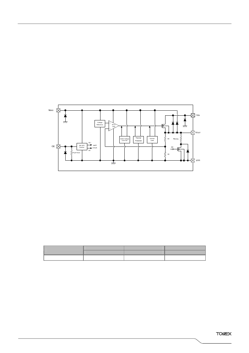
The voltage divided by resistors R1 & R2 is compared with the internal reference voltage by the error amplifier. The P-channel
MOSFET which is connected to the V
OUT
pin is then driven by the subsequent output signal. The output voltage at the V
OUT
pin is
controlled & stabilized by a system of negative feedback.
V
BIAS
pin is power supply pin for output voltage control circuit, protection circuit and CE circuit. When output current increase,
the V
BIAS
pin supplies output current also. VIN pin is connected to a driver transistor and provides output current.
In order to obtain high efficient output current through low on-resistance, please take enough Vgs (=V
BIAS
– V
OUT
) of the driver
transistor. Output current triggers operation of constant current limiter and foldback circuit, heat generation triggers operation of
thermal shutdown circuit, the driver transistor circuit is forced OFF when V
BIAS
or V
IN
voltage goes lower than U.V.L.O. voltage.
Further, the IC's internal circuitry can be shutdown via the CE pin's signal.
XC6601A series
<
Low ESR Capacitor
>
With the XC6601 series, a stable output voltage is achievable even if used with low ESR capacitors, as a phase compensation
circuit is built-in. The output capacitor (C
L
) should be connected as close to V
OUT
pin and V
SS
pin to obtain stable phase
compensation. Values required for the phase compensation are as the table below.
For a stable power input, please connect an bias capacitor (C
BIAS
) of 1.0
please connect an input capacitor (C
IN
) of 1.0
F between the V
IN
pin and the V
SS
pin. In order to ensure the stable phase
compensation while avoiding run-out of values, please use the capacitor (C
BIAS
, C
IN
, C
L
) which does not depend on bias or
temperature too much. The table below shows recommended values of C
BIAS
, C
IN
, C
L
.
F between the V
BIAS
pin and the V
SS
pin. Also,
Recommended Values of C
BIAS,
C
IN,
C
L
BIAS CAPACITOR
C
BIAS
C
BIAS
=1.0μF
INPUT CAPACITOR
C
IN
C
IN
=1.0μF
OUTPUT CAPACITOR
C
L
C
L
=4.7μF
SETTING VOLTAGE
0.7V~1.8V
OPERATIONAL EXPLANATION
相關(guān)PDF資料 |
PDF描述 |
|---|---|
| XC66DC2550ML | Analog IC |
| XC66DC2550MR | Analog IC |
| XC66DC3833ML | Analog IC |
| XC66DC3850ML | Analog IC |
| XC66DC3850MR | Analog IC |
相關(guān)代理商/技術(shù)參數(shù) |
參數(shù)描述 |
|---|---|
| XC6601_1 | 制造商:TOREX 制造商全稱:Torex Semiconductor 功能描述:Low Voltage Input LDO Voltage Regulators |
| XC6601_2 | 制造商:TOREX 制造商全稱:Torex Semiconductor 功能描述:Low Voltage Input LDO Voltage Regulator with Soft-Start Function |
| XC6601A071EL | 制造商:TOREX 制造商全稱:Torex Semiconductor 功能描述:Low Voltage Input LDO Voltage Regulators |
| XC6601A071ER | 制造商:TOREX 制造商全稱:Torex Semiconductor 功能描述:Low Voltage Input LDO Voltage Regulators |
| XC6601A071ER-G | 制造商:TOREX 制造商全稱:Torex Semiconductor 功能描述:Low Voltage Input LDO Voltage Regulator with Soft-Start Function |
發(fā)布緊急采購,3分鐘左右您將得到回復(fù)。