- 您現(xiàn)在的位置:買賣IC網(wǎng) > PDF目錄4172 > XC4003E-1PG120C (Xilinx Inc)IC FPGA C-TEMP 5V 1-SPD 120-CPGA PDF資料下載
參數(shù)資料
| 型號: | XC4003E-1PG120C |
| 廠商: | Xilinx Inc |
| 文件頁數(shù): | 35/68頁 |
| 文件大?。?/td> | 0K |
| 描述: | IC FPGA C-TEMP 5V 1-SPD 120-CPGA |
| 產(chǎn)品變化通告: | XC4000(E,L) Discontinuation 01/April/2002 |
| 標(biāo)準(zhǔn)包裝: | 24 |
| 系列: | XC4000E/X |
| LAB/CLB數(shù): | 100 |
| 邏輯元件/單元數(shù): | 238 |
| RAM 位總計: | 3200 |
| 輸入/輸出數(shù): | 80 |
| 門數(shù): | 3000 |
| 電源電壓: | 4.75 V ~ 5.25 V |
| 安裝類型: | 表面貼裝 |
| 工作溫度: | 0°C ~ 85°C |
| 封裝/外殼: | 120-BCBGA |
| 供應(yīng)商設(shè)備封裝: | 120-CPGA(34.55x34.55) |
第1頁第2頁第3頁第4頁第5頁第6頁第7頁第8頁第9頁第10頁第11頁第12頁第13頁第14頁第15頁第16頁第17頁第18頁第19頁第20頁第21頁第22頁第23頁第24頁第25頁第26頁第27頁第28頁第29頁第30頁第31頁第32頁第33頁第34頁當(dāng)前第35頁第36頁第37頁第38頁第39頁第40頁第41頁第42頁第43頁第44頁第45頁第46頁第47頁第48頁第49頁第50頁第51頁第52頁第53頁第54頁第55頁第56頁第57頁第58頁第59頁第60頁第61頁第62頁第63頁第64頁第65頁第66頁第67頁第68頁
R
XC4000E and XC4000X Series Field Programmable Gate Arrays
6-44
May 14, 1999 (Version 1.6)
Instruction Set
The XC4000 Series boundary scan instruction set also
includes instructions to congure the device and read back
the conguration data. The instruction set is coded as
shown in Table 17.
Bit Sequence
The bit sequence within each IOB is: In, Out, 3-State. The
input-only M0 and M2 mode pins contribute only the In bit
to the boundary scan I/O data register, while the out-
put-only M1 pin contributes all three bits.
The rst two bits in the I/O data register are TDO.T and
TDO.O, which can be used for the capture of internal sig-
nals. The nal bit is BSCANT.UPD, which can be used to
drive an internal net. These locations are primarily used by
Xilinx for internal testing.
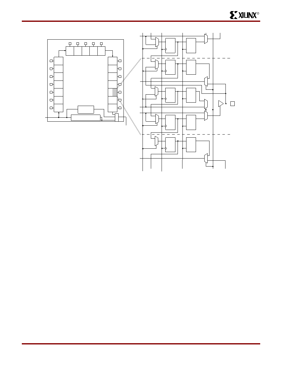
From a cavity-up view of the chip (as shown in XDE or
Epic), starting in the upper right chip corner, the boundary
scan data-register bits are ordered as shown in Figure 42.
The device-specic pinout tables for the XC4000 Series
include the boundary scan locations for each IOB pin.
BSDL (Boundary Scan Description Language) les for
XC4000 Series devices are available on the Xilinx FTP site.
Including Boundary Scan in a Schematic
If boundary scan is only to be used during conguration, no
special schematic elements need be included in the sche-
matic or HDL code. In this case, the special boundary scan
pins TDI, TMS, TCK and TDO can be used for user func-
tions after conguration.
To indicate that boundary scan remain enabled after cong-
uration, place the BSCAN library symbol and connect the
TDI, TMS, TCK and TDO pad symbols to the appropriate
pins, as shown in Figure 43.
Even if the boundary scan symbol is used in a schematic,
the input pins TMS, TCK, and TDI can still be used as
inputs to be routed to internal logic. Care must be taken not
to force the chip into an undesired boundary scan state by
inadvertently applying boundary scan input patterns to
these pins. The simplest way to prevent this is to keep TMS
High, and then apply whatever signal is desired to TDI and
TCK.
D
Q
D
Q
IOB
M
U
X
BYPASS
REGISTER
IOB
TDO
TDI
IOB
1
0
1
0
1
0
1
0
1
0
sd
LE
DQ
D
Q
D
Q
1
0
1
0
1
0
1
0
DQ
LE
sd
LE
DQ
sd
LE
DQ
IOB
D
Q
1
0
DQ
LE
sd
IOB.T
DATA IN
IOB.I
IOB.Q
IOB.T
IOB.I
SHIFT/
CAPTURE
CLOCK DATA
REGISTER
DATAOUT
UPDATE
EXTEST
X9016
INSTRUCTION REGISTER
Figure 41: XC4000 Series Boundary Scan Logic
Product Obsolete or Under Obsolescence
相關(guān)PDF資料 |
PDF描述 |
|---|---|
| XC4003E-1PC84C | IC FPGA C-TEMP 5V 1-SPD 84-PLCC |
| XC3090L-8PC84I | IC FPGA 3.3V I-TEMP 84-PLCC |
| FMC18DREN-S13 | CONN EDGECARD 36POS .100 EXTEND |
| FMC18DREH-S13 | CONN EDGECARD 36POS .100 EXTEND |
| FMM28DSEF | CONN EDGECARD 56POS .156 EYELET |
相關(guān)代理商/技術(shù)參數(shù) |
參數(shù)描述 |
|---|---|
| XC4003E-1PG120I | 制造商:未知廠家 制造商全稱:未知廠家 功能描述:Field Programmable Gate Array (FPGA) |
| XC4003E-1PG120M | 制造商:未知廠家 制造商全稱:未知廠家 功能描述:Field Programmable Gate Array (FPGA) |
| XC4003E-1PQ100C | 功能描述:IC FPGA C-TEMP 5V 1-SPD 100-PQFP RoHS:否 類別:集成電路 (IC) >> 嵌入式 - FPGA(現(xiàn)場可編程門陣列) 系列:XC4000E/X 產(chǎn)品變化通告:XC4000(E,L) Discontinuation 01/April/2002 標(biāo)準(zhǔn)包裝:24 系列:XC4000E/X LAB/CLB數(shù):100 邏輯元件/單元數(shù):238 RAM 位總計:3200 輸入/輸出數(shù):80 門數(shù):3000 電源電壓:4.5 V ~ 5.5 V 安裝類型:表面貼裝 工作溫度:-40°C ~ 100°C 封裝/外殼:120-BCBGA 供應(yīng)商設(shè)備封裝:120-CPGA(34.55x34.55) |
| XC4003E-1PQ100I | 制造商:未知廠家 制造商全稱:未知廠家 功能描述:Field Programmable Gate Array (FPGA) |
| XC4003E-1VQ100C | 功能描述:IC FPGA C-TEMP 5V 1SPD 100-VQFP RoHS:否 類別:集成電路 (IC) >> 嵌入式 - FPGA(現(xiàn)場可編程門陣列) 系列:XC4000E/X 產(chǎn)品變化通告:XC4000(E,L) Discontinuation 01/April/2002 標(biāo)準(zhǔn)包裝:24 系列:XC4000E/X LAB/CLB數(shù):100 邏輯元件/單元數(shù):238 RAM 位總計:3200 輸入/輸出數(shù):80 門數(shù):3000 電源電壓:4.5 V ~ 5.5 V 安裝類型:表面貼裝 工作溫度:-40°C ~ 100°C 封裝/外殼:120-BCBGA 供應(yīng)商設(shè)備封裝:120-CPGA(34.55x34.55) |
發(fā)布緊急采購,3分鐘左右您將得到回復(fù)。