- 您現(xiàn)在的位置:買賣IC網(wǎng) > PDF目錄4127 > XC3S4000L-4FGG900C (Xilinx Inc)SPARTAN-3A FPGA 4M STD 900-FBGA PDF資料下載
參數(shù)資料
| 型號(hào): | XC3S4000L-4FGG900C |
| 廠商: | Xilinx Inc |
| 文件頁(yè)數(shù): | 20/272頁(yè) |
| 文件大小: | 0K |
| 描述: | SPARTAN-3A FPGA 4M STD 900-FBGA |
| 產(chǎn)品變化通告: | Product Discontinuation Notice 14/May/2007 |
| 標(biāo)準(zhǔn)包裝: | 1 |
| 系列: | Spartan®-3 |
| LAB/CLB數(shù): | 1728 |
| 邏輯元件/單元數(shù): | 62208 |
| RAM 位總計(jì): | 1769472 |
| 輸入/輸出數(shù): | 633 |
| 門數(shù): | 4000000 |
| 電源電壓: | 1.14 V ~ 1.26 V |
| 安裝類型: | 表面貼裝 |
| 工作溫度: | 0°C ~ 85°C |
| 封裝/外殼: | 900-BBGA |
| 供應(yīng)商設(shè)備封裝: | 900-FBGA |
第1頁(yè)第2頁(yè)第3頁(yè)第4頁(yè)第5頁(yè)第6頁(yè)第7頁(yè)第8頁(yè)第9頁(yè)第10頁(yè)第11頁(yè)第12頁(yè)第13頁(yè)第14頁(yè)第15頁(yè)第16頁(yè)第17頁(yè)第18頁(yè)第19頁(yè)當(dāng)前第20頁(yè)第21頁(yè)第22頁(yè)第23頁(yè)第24頁(yè)第25頁(yè)第26頁(yè)第27頁(yè)第28頁(yè)第29頁(yè)第30頁(yè)第31頁(yè)第32頁(yè)第33頁(yè)第34頁(yè)第35頁(yè)第36頁(yè)第37頁(yè)第38頁(yè)第39頁(yè)第40頁(yè)第41頁(yè)第42頁(yè)第43頁(yè)第44頁(yè)第45頁(yè)第46頁(yè)第47頁(yè)第48頁(yè)第49頁(yè)第50頁(yè)第51頁(yè)第52頁(yè)第53頁(yè)第54頁(yè)第55頁(yè)第56頁(yè)第57頁(yè)第58頁(yè)第59頁(yè)第60頁(yè)第61頁(yè)第62頁(yè)第63頁(yè)第64頁(yè)第65頁(yè)第66頁(yè)第67頁(yè)第68頁(yè)第69頁(yè)第70頁(yè)第71頁(yè)第72頁(yè)第73頁(yè)第74頁(yè)第75頁(yè)第76頁(yè)第77頁(yè)第78頁(yè)第79頁(yè)第80頁(yè)第81頁(yè)第82頁(yè)第83頁(yè)第84頁(yè)第85頁(yè)第86頁(yè)第87頁(yè)第88頁(yè)第89頁(yè)第90頁(yè)第91頁(yè)第92頁(yè)第93頁(yè)第94頁(yè)第95頁(yè)第96頁(yè)第97頁(yè)第98頁(yè)第99頁(yè)第100頁(yè)第101頁(yè)第102頁(yè)第103頁(yè)第104頁(yè)第105頁(yè)第106頁(yè)第107頁(yè)第108頁(yè)第109頁(yè)第110頁(yè)第111頁(yè)第112頁(yè)第113頁(yè)第114頁(yè)第115頁(yè)第116頁(yè)第117頁(yè)第118頁(yè)第119頁(yè)第120頁(yè)第121頁(yè)第122頁(yè)第123頁(yè)第124頁(yè)第125頁(yè)第126頁(yè)第127頁(yè)第128頁(yè)第129頁(yè)第130頁(yè)第131頁(yè)第132頁(yè)第133頁(yè)第134頁(yè)第135頁(yè)第136頁(yè)第137頁(yè)第138頁(yè)第139頁(yè)第140頁(yè)第141頁(yè)第142頁(yè)第143頁(yè)第144頁(yè)第145頁(yè)第146頁(yè)第147頁(yè)第148頁(yè)第149頁(yè)第150頁(yè)第151頁(yè)第152頁(yè)第153頁(yè)第154頁(yè)第155頁(yè)第156頁(yè)第157頁(yè)第158頁(yè)第159頁(yè)第160頁(yè)第161頁(yè)第162頁(yè)第163頁(yè)第164頁(yè)第165頁(yè)第166頁(yè)第167頁(yè)第168頁(yè)第169頁(yè)第170頁(yè)第171頁(yè)第172頁(yè)第173頁(yè)第174頁(yè)第175頁(yè)第176頁(yè)第177頁(yè)第178頁(yè)第179頁(yè)第180頁(yè)第181頁(yè)第182頁(yè)第183頁(yè)第184頁(yè)第185頁(yè)第186頁(yè)第187頁(yè)第188頁(yè)第189頁(yè)第190頁(yè)第191頁(yè)第192頁(yè)第193頁(yè)第194頁(yè)第195頁(yè)第196頁(yè)第197頁(yè)第198頁(yè)第199頁(yè)第200頁(yè)第201頁(yè)第202頁(yè)第203頁(yè)第204頁(yè)第205頁(yè)第206頁(yè)第207頁(yè)第208頁(yè)第209頁(yè)第210頁(yè)第211頁(yè)第212頁(yè)第213頁(yè)第214頁(yè)第215頁(yè)第216頁(yè)第217頁(yè)第218頁(yè)第219頁(yè)第220頁(yè)第221頁(yè)第222頁(yè)第223頁(yè)第224頁(yè)第225頁(yè)第226頁(yè)第227頁(yè)第228頁(yè)第229頁(yè)第230頁(yè)第231頁(yè)第232頁(yè)第233頁(yè)第234頁(yè)第235頁(yè)第236頁(yè)第237頁(yè)第238頁(yè)第239頁(yè)第240頁(yè)第241頁(yè)第242頁(yè)第243頁(yè)第244頁(yè)第245頁(yè)第246頁(yè)第247頁(yè)第248頁(yè)第249頁(yè)第250頁(yè)第251頁(yè)第252頁(yè)第253頁(yè)第254頁(yè)第255頁(yè)第256頁(yè)第257頁(yè)第258頁(yè)第259頁(yè)第260頁(yè)第261頁(yè)第262頁(yè)第263頁(yè)第264頁(yè)第265頁(yè)第266頁(yè)第267頁(yè)第268頁(yè)第269頁(yè)第270頁(yè)第271頁(yè)第272頁(yè)
Spartan-3 FPGA Family: Pinout Descriptions
DS099 (v3.1) June 27, 2013
Product Specification
116
The 1% precision impedance-matching resistor attached to the VRN_# pin controls the pull-down impedance of NMOS
transistor in the input or output buffer. Consequently, the VRN_# pin must connect to VCCO. The ‘N’ character in “VRN”
indicates that this pin controls the I/O buffer’s NMOS transistor impedance. The VRN_# pin is only used for split termination.
Each VRN or VRP reference input requires its own resistor. A single resistor cannot be shared between VRN or VRP pins
associated with different banks.
During configuration, these pins behave exactly like user-I/O pins. The associated DCI behavior is not active or valid until
after configuration completes.
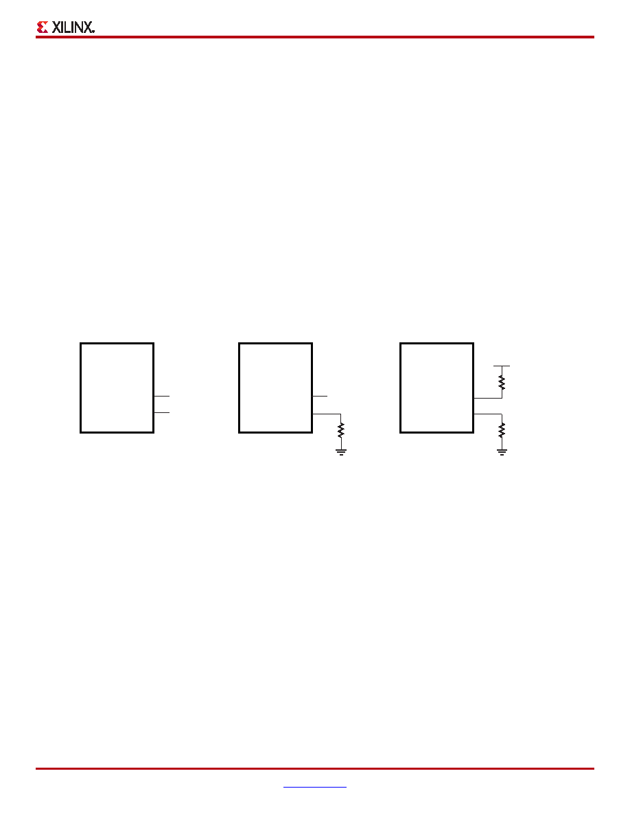
DCI Termination Types
If the I/O in an I/O bank do not use the DCI feature, then no external resistors are required and both the VRP_# and VRN_#
pins are available for user I/O, as shown in section [a] of Figure 42.
If the I/O standards within the associated I/O bank require single termination—such as GTL_DCI, GTLP_DCI, or
HSTL_III_DCI—then only the VRP_# signal connects to a 1% precision impedance-matching resistor, as shown in section
[b] of Figure 42. A resistor is not required for the VRN_# pin.
Finally, if the I/O standards with the associated I/O bank require split termination—such as HSTL_I_DCI, SSTL2_I_DCI,
SSTL2_II_DCI, or LVDS_25_DCI and LVDSEXT_25_DCI receivers—then both the VRP_# and VRN_# pins connect to
separate 1% precision impedance-matching resistors, as shown in section [c] of Figure 42. Neither pin is available for user
I/O.
GCLK: Global Clock Buffer Inputs or General-Purpose I/O Pins
These pins are user-I/O pins unless they specifically connect to one of the eight low-skew global clock buffers on the device,
specified using the IBUFG primitive.
There are eight GCLK pins per device and two each appear in the top-edge banks, Bank 0 and 1, and the bottom-edge
banks, Banks 4 and 5. See Figure 40 for a picture of bank labeling.
During configuration, these pins behave exactly like user-I/O pins.
Also see Global Clock Network, page 42.
CONFIG: Dedicated Configuration Pins
The dedicated configuration pins control the configuration process and are not available as user-I/O pins. Every package
has seven dedicated configuration pins. All CONFIG-type pins are powered by the +2.5V VCCAUX supply.
Also see Configuration, page 46.
X-Ref Target - Figure 42
Figure 42: DCI Termination Types
DS099-4_03_091910
VCCO
VRN
VRP
One of eight
I/O Banks
RREF (1%)
(c) Split termination
VRN
VRP
One of eight
I/O Banks
RREF (1%)
(b) Single termination
User I/O
One of eight
I/O Banks
(a) No termination
相關(guān)PDF資料 |
PDF描述 |
|---|---|
| AMM36DRMD-S288 | CONN EDGECARD 72POS .156 EXTEND |
| FMC20DRES | CONN EDGECARD 40POS .100 EYELET |
| IDT71342LA55PF8 | IC SRAM 32KBIT 55NS 64TQFP |
| IDT71421SA35PF8 | IC SRAM 16KBIT 35NS 64TQFP |
| IDT71321SA35PF8 | IC SRAM 16KBIT 35NS 64TQFP |
相關(guān)代理商/技術(shù)參數(shù) |
參數(shù)描述 |
|---|---|
| XC3S400-4CP132C | 制造商:XILINX 制造商全稱:XILINX 功能描述:Spartan-3 FPGA Family: Complete Data Sheet |
| XC3S400-4CP132I | 制造商:XILINX 制造商全稱:XILINX 功能描述:Spartan-3 FPGA Family: Complete Data Sheet |
| XC3S400-4CPG132C | 制造商:XILINX 制造商全稱:XILINX 功能描述:Spartan-3 FPGA Family: Complete Data Sheet |
| XC3S400-4CPG132I | 制造商:XILINX 制造商全稱:XILINX 功能描述:Spartan-3 FPGA Family: Complete Data Sheet |
| XC3S400-4FG1156C | 制造商:XILINX 制造商全稱:XILINX 功能描述:Spartan-3 FPGA Family : Complete Data Sheet |
發(fā)布緊急采購(gòu),3分鐘左右您將得到回復(fù)。