- 您現在的位置:買賣IC網 > PDF目錄21990 > XC3S100E-4VQG100C (Xilinx Inc)IC SPARTAN-3E FPGA 100K 100VTQFP PDF資料下載
參數資料
| 型號: | XC3S100E-4VQG100C |
| 廠商: | Xilinx Inc |
| 文件頁數: | 164/227頁 |
| 文件大小: | 0K |
| 描述: | IC SPARTAN-3E FPGA 100K 100VTQFP |
| 產品培訓模塊: | FPGAs Spartan3 |
| 標準包裝: | 90 |
| 系列: | Spartan®-3E |
| LAB/CLB數: | 240 |
| 邏輯元件/單元數: | 2160 |
| RAM 位總計: | 73728 |
| 輸入/輸出數: | 66 |
| 門數: | 100000 |
| 電源電壓: | 1.14 V ~ 1.26 V |
| 安裝類型: | 表面貼裝 |
| 工作溫度: | 0°C ~ 85°C |
| 封裝/外殼: | 100-TQFP |
| 供應商設備封裝: | 100-VQFP(14x14) |
| 產品目錄頁面: | 599 (CN2011-ZH PDF) |
| 其它名稱: | 122-1479 |
第1頁第2頁第3頁第4頁第5頁第6頁第7頁第8頁第9頁第10頁第11頁第12頁第13頁第14頁第15頁第16頁第17頁第18頁第19頁第20頁第21頁第22頁第23頁第24頁第25頁第26頁第27頁第28頁第29頁第30頁第31頁第32頁第33頁第34頁第35頁第36頁第37頁第38頁第39頁第40頁第41頁第42頁第43頁第44頁第45頁第46頁第47頁第48頁第49頁第50頁第51頁第52頁第53頁第54頁第55頁第56頁第57頁第58頁第59頁第60頁第61頁第62頁第63頁第64頁第65頁第66頁第67頁第68頁第69頁第70頁第71頁第72頁第73頁第74頁第75頁第76頁第77頁第78頁第79頁第80頁第81頁第82頁第83頁第84頁第85頁第86頁第87頁第88頁第89頁第90頁第91頁第92頁第93頁第94頁第95頁第96頁第97頁第98頁第99頁第100頁第101頁第102頁第103頁第104頁第105頁第106頁第107頁第108頁第109頁第110頁第111頁第112頁第113頁第114頁第115頁第116頁第117頁第118頁第119頁第120頁第121頁第122頁第123頁第124頁第125頁第126頁第127頁第128頁第129頁第130頁第131頁第132頁第133頁第134頁第135頁第136頁第137頁第138頁第139頁第140頁第141頁第142頁第143頁第144頁第145頁第146頁第147頁第148頁第149頁第150頁第151頁第152頁第153頁第154頁第155頁第156頁第157頁第158頁第159頁第160頁第161頁第162頁第163頁當前第164頁第165頁第166頁第167頁第168頁第169頁第170頁第171頁第172頁第173頁第174頁第175頁第176頁第177頁第178頁第179頁第180頁第181頁第182頁第183頁第184頁第185頁第186頁第187頁第188頁第189頁第190頁第191頁第192頁第193頁第194頁第195頁第196頁第197頁第198頁第199頁第200頁第201頁第202頁第203頁第204頁第205頁第206頁第207頁第208頁第209頁第210頁第211頁第212頁第213頁第214頁第215頁第216頁第217頁第218頁第219頁第220頁第221頁第222頁第223頁第224頁第225頁第226頁第227頁
Spartan-3E FPGA Family: Functional Description
DS312 (v4.1) July 19, 2013
Product Specification
41
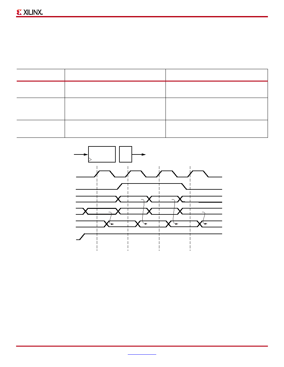
There are a number of different conditions under which data
can be accessed at the DO outputs. Basic data access
always occurs when the WE input is inactive. Under this
condition, data stored in the memory location addressed by
the ADDR lines passes through a output latch to the DO
outputs. The timing for basic data access is shown in the
which WE is Low.
Data also can be accessed on the DO outputs when
asserting the WE input based on the value of the
WRITE_MODE attribute as described in Table 26.
Setting the WRITE_MODE attribute to a value of
WRITE_FIRST, data is written to the addressed memory
location on an enabled active CLK edge and is also passed
to the DO outputs. WRITE_FIRST timing is shown in the
portion of Figure 33 during which WE is High.
Setting the WRITE_MODE attribute to a value of
READ_FIRST, data already stored in the addressed
location passes to the DO outputs before that location is
overwritten with new data from the DI inputs on an enabled
active CLK edge. READ_FIRST timing is shown in the
portion of Figure 34 during which WE is High.
Table 26: WRITE_MODE Effect on Data Output Latches During Write Operations
Write Mode
Effect on Same Port
Effect on Opposite Port
(dual-port only with same address)
WRITE_FIRST
Read After Write
Data on DI and DIP inputs is written into specified
RAM location and simultaneously appears on DO and
DOP outputs.
Invalidates data on DO and DOP outputs.
READ_FIRST
Read Before Write
Data from specified RAM location appears on DO and
DOP outputs.
Data on DI and DIP inputs is written into specified
location.
Data from specified RAM location appears on DO and
DOP outputs.
NO_CHANGE
No Read on Write
Data on DO and DOP outputs remains unchanged.
Data on DI and DIP inputs is written into specified
location.
Invalidates data on DO and DOP outputs.
X-Ref Target - Figure 33
Figure 33: Waveforms of Block RAM Data Operations with WRITE_FIRST Selected
CLK
WE
DI
ADDR
DO
EN
DISABLED
READ
XXXX
1111
2222
XXXX
aa
bb
cc
dd
0000
MEM(aa)
1111
2222
MEM(dd)
READ
WRITE
MEM(bb)=1111
WRITE
MEM(cc)=2222
DS312-2_05_020905
Data_in
Internal
Memory
DO
Data_out = Data_in
DI
相關PDF資料 |
PDF描述 |
|---|---|
| VI-B60-CW | CONVERTER MOD DC/DC 5V 100W |
| VI-27M-CW-F1 | CONVERTER MOD DC/DC 10V 100W |
| VI-B5H-CX | CONVERTER MOD DC/DC 52V 75W |
| XC3S50-4VQG100C | IC SPARTAN-3 FPGA 50K 100VTQFP |
| VI-B5F-CX | CONVERTER MOD DC/DC 72V 75W |
相關代理商/技術參數 |
參數描述 |
|---|---|
| XC3S100E-4VQG100I | 功能描述:IC FPGA SPARTAN-3E 100K 100-VQFP RoHS:是 類別:集成電路 (IC) >> 嵌入式 - FPGA(現場可編程門陣列) 系列:Spartan®-3E 標準包裝:40 系列:Spartan® 6 LX LAB/CLB數:3411 邏輯元件/單元數:43661 RAM 位總計:2138112 輸入/輸出數:358 門數:- 電源電壓:1.14 V ~ 1.26 V 安裝類型:表面貼裝 工作溫度:-40°C ~ 100°C 封裝/外殼:676-BGA 供應商設備封裝:676-FBGA(27x27) |
| XC3S100E-5CP132C | 制造商:Xilinx 功能描述:FPGA SPARTAN-3E 100K GATES 2160 CELLS 657MHZ COMM 90NM 1.2V - Trays |
| XC3S100E-5CP132GC | 制造商:XILINX 制造商全稱:XILINX 功能描述:Spartan-3E FPGA Family: Complete Data Sheet |
| XC3S100E-5CP132GI | 制造商:XILINX 制造商全稱:XILINX 功能描述:Spartan-3E FPGA Family: Complete Data Sheet |
| XC3S100E-5CP132I | 制造商:XILINX 制造商全稱:XILINX 功能描述:Spartan-3E FPGA Family: Complete Data Sheet |
發(fā)布緊急采購,3分鐘左右您將得到回復。