- 您現(xiàn)在的位置:買賣IC網(wǎng) > PDF目錄374985 > XC3S1000-4FG900I (XILINX INC) Spartan-3 FPGA Family : Complete Data Sheet PDF資料下載
參數(shù)資料
| 型號(hào): | XC3S1000-4FG900I |
| 廠商: | XILINX INC |
| 元件分類: | FPGA |
| 英文描述: | Spartan-3 FPGA Family : Complete Data Sheet |
| 中文描述: | FPGA, 192 CLBS, 50000 GATES, PBGA900 |
| 封裝: | FBGA-900 |
| 文件頁(yè)數(shù): | 11/192頁(yè) |
| 文件大小: | 1555K |
| 代理商: | XC3S1000-4FG900I |
第1頁(yè)第2頁(yè)第3頁(yè)第4頁(yè)第5頁(yè)第6頁(yè)第7頁(yè)第8頁(yè)第9頁(yè)第10頁(yè)當(dāng)前第11頁(yè)第12頁(yè)第13頁(yè)第14頁(yè)第15頁(yè)第16頁(yè)第17頁(yè)第18頁(yè)第19頁(yè)第20頁(yè)第21頁(yè)第22頁(yè)第23頁(yè)第24頁(yè)第25頁(yè)第26頁(yè)第27頁(yè)第28頁(yè)第29頁(yè)第30頁(yè)第31頁(yè)第32頁(yè)第33頁(yè)第34頁(yè)第35頁(yè)第36頁(yè)第37頁(yè)第38頁(yè)第39頁(yè)第40頁(yè)第41頁(yè)第42頁(yè)第43頁(yè)第44頁(yè)第45頁(yè)第46頁(yè)第47頁(yè)第48頁(yè)第49頁(yè)第50頁(yè)第51頁(yè)第52頁(yè)第53頁(yè)第54頁(yè)第55頁(yè)第56頁(yè)第57頁(yè)第58頁(yè)第59頁(yè)第60頁(yè)第61頁(yè)第62頁(yè)第63頁(yè)第64頁(yè)第65頁(yè)第66頁(yè)第67頁(yè)第68頁(yè)第69頁(yè)第70頁(yè)第71頁(yè)第72頁(yè)第73頁(yè)第74頁(yè)第75頁(yè)第76頁(yè)第77頁(yè)第78頁(yè)第79頁(yè)第80頁(yè)第81頁(yè)第82頁(yè)第83頁(yè)第84頁(yè)第85頁(yè)第86頁(yè)第87頁(yè)第88頁(yè)第89頁(yè)第90頁(yè)第91頁(yè)第92頁(yè)第93頁(yè)第94頁(yè)第95頁(yè)第96頁(yè)第97頁(yè)第98頁(yè)第99頁(yè)第100頁(yè)第101頁(yè)第102頁(yè)第103頁(yè)第104頁(yè)第105頁(yè)第106頁(yè)第107頁(yè)第108頁(yè)第109頁(yè)第110頁(yè)第111頁(yè)第112頁(yè)第113頁(yè)第114頁(yè)第115頁(yè)第116頁(yè)第117頁(yè)第118頁(yè)第119頁(yè)第120頁(yè)第121頁(yè)第122頁(yè)第123頁(yè)第124頁(yè)第125頁(yè)第126頁(yè)第127頁(yè)第128頁(yè)第129頁(yè)第130頁(yè)第131頁(yè)第132頁(yè)第133頁(yè)第134頁(yè)第135頁(yè)第136頁(yè)第137頁(yè)第138頁(yè)第139頁(yè)第140頁(yè)第141頁(yè)第142頁(yè)第143頁(yè)第144頁(yè)第145頁(yè)第146頁(yè)第147頁(yè)第148頁(yè)第149頁(yè)第150頁(yè)第151頁(yè)第152頁(yè)第153頁(yè)第154頁(yè)第155頁(yè)第156頁(yè)第157頁(yè)第158頁(yè)第159頁(yè)第160頁(yè)第161頁(yè)第162頁(yè)第163頁(yè)第164頁(yè)第165頁(yè)第166頁(yè)第167頁(yè)第168頁(yè)第169頁(yè)第170頁(yè)第171頁(yè)第172頁(yè)第173頁(yè)第174頁(yè)第175頁(yè)第176頁(yè)第177頁(yè)第178頁(yè)第179頁(yè)第180頁(yè)第181頁(yè)第182頁(yè)第183頁(yè)第184頁(yè)第185頁(yè)第186頁(yè)第187頁(yè)第188頁(yè)第189頁(yè)第190頁(yè)第191頁(yè)第192頁(yè)
Spartan-3 1.2V FPGA Family: Functional Description
4
www.xilinx.com
1-800-255-7778
DS099-2 (v1.2) July 11, 2003
Advance Product Specification
40
R
Pull-Up and Pull-Down Resistors
The optional pull-up and pull-down resistors are intended to
establish High and Low levels, respectively, at unused I/Os.
The weak pull-up resistor optionally connects each IOB pad
to V
CCO
. A weak pull-down resistor optionally connects
each pad to GND. These resistors are placed in a design
using the PULLUP and PULLDOWN symbols in a sche-
matic, respectively. They can also be instantiated as com-
ponents, set as constraints or passed as attributes in HDL
code. These resistors can also be selected for all unused
I/O using the Bitstream Generator (BitGen) option Unused-
Pin. A Low logic level on HSWAP_EN activates the pull-up
resistors on all I/Os during configuration.
Weak-Keeper Circuit
Each I/O has an optional weak-keeper circuit that retains
the last logic level on a line after all drivers have been turned
off. This is useful to keep bus lines from floating when all
connected drivers are in a high-impedance state. This func-
tion is placed in a design using the KEEPER symbol.
Pull-up and pull-down resistors override the weak-keeper
circuit.
ESD Protection
Clamp diodes protect all device pads against damage from
Electro-Static Discharge (ESD) as well as excessive voltage
transients. Each I/O has two clamp diodes: One diode
extends P-to-N from the pad to V
CCO
and a second diode
extends N-to-P from the pad to GND. During operation,
these diodes are normally biased in the off state. These
clamp diodes are always connected to the pad, regardless
of the signal standard selected. The presence of diodes lim-
its the ability of Spartan-3 I/Os to tolerate high signal volt-
ages. The V
IN
absolute maximum rating in
Table 1
in
Module 3:
DC and Switching Characteristics
specifies the
voltage range that I/Os can tolerate.
Slew Rate Control and Drive Strength
Two options, FAST and SLOW, control the output slew rate.
The FAST option supports output switching at a high rate.
The SLOW option reduces bus transients. These options are
only available when using one of the LVCMOS or LVTTL
standards, which also provide up to seven different levels of
current drive strength: 2, 4, 6, 8, 12, 16, and 24 mA. Choos-
ing the appropriate drive strength level is yet another means
to minimize bus transients.
Table 3
shows the drive strengths that the LVCMOS and
LVTTL standards support. The Fast option is indicated by
appending an "F" attribute after the output buffer symbol
OBUF or the bidirectional buffer symbol IOBUF. The Slow
option appends an "S" attribute. The drive strength in milliam-
peres follows the slew rate attribute. For example,
OBUF_LVCMOS18_S_6 or IOBUF_LVCMOS25_F_16.
Boundary-Scan Capability
All Spartan-3 IOBs support boundary-scan testing compat-
ible with IEEE 1149.1 standards. See
Boundary-Scan
(JTAG) Mode
, page 36
for more information.
SelectIO
Signal Standards
The IOBs support 17 different single-ended signal stan-
dards, as listed in
Table 4
. Furthermore, the majority of
IOBs can be used in specific pairs supporting any of six dif-
ferential signal standards, as shown in
Table 5
. The desired
standard is selected by placing the appropriate I/O library
symbol or component into the FPGA design. For example,
the symbol named IOBUF_LVCMOS15_F_8 represents a
bidirectional I/O to which the 1.5V LVCMOS signal standard
has been assigned. The slew rate and current drive are set
to Fast and 8 mA, respectively.
Together with placing the appropriate I/O symbol, two exter-
nally applied voltage levels, V
CCO
and V
REF
select the
desired signal standard. The V
CCO
lines provide current to
the output driver. The voltage on these lines determines the
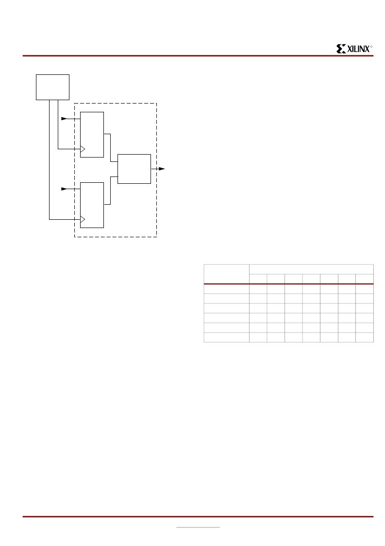
Figure 2:
Clocking the DDR Register
D1
CLK1
DDR MUX
DCM
Q1
FDDR
D2
CLK2
Q2
180 0
DS099-2_02_070303
Q
Table 3:
Programmable Output Drive Current
Signal
Standard
LVCMOS12
LVCMOS15
LVCMOS18
LVCMOS25
LVCMOS33
LVTTL
Current Drive (mA)
6
8
3
-
3
3
3
3
3
3
3
3
3
3
2
3
3
3
3
3
3
4
3
3
3
3
3
3
12
-
3
3
3
3
3
16
-
-
3
3
3
3
24
-
-
-
3
3
3
相關(guān)PDF資料 |
PDF描述 |
|---|---|
| XC3S1000-4FT256C | Spartan-3 FPGA Family : Complete Data Sheet |
| XC3S1000-4FT256I | Spartan-3 FPGA Family : Complete Data Sheet |
| XC3S1000-4TQ144C | Spartan-3 FPGA Family: Complete Data Sheet |
| XC3S1000 | Spartan-3 FPGA Family: Complete Data Sheet |
| XC3S1000-4CP132C | Spartan-3 FPGA Family: Complete Data Sheet |
相關(guān)代理商/技術(shù)參數(shù) |
參數(shù)描述 |
|---|---|
| XC3S1000-4FGG320C | 功能描述:SPARTAN-3A FPGA 1M STD 320-FBGA RoHS:是 類別:集成電路 (IC) >> 嵌入式 - FPGA(現(xiàn)場(chǎng)可編程門陣列) 系列:Spartan®-3 標(biāo)準(zhǔn)包裝:40 系列:Spartan® 6 LX LAB/CLB數(shù):3411 邏輯元件/單元數(shù):43661 RAM 位總計(jì):2138112 輸入/輸出數(shù):358 門數(shù):- 電源電壓:1.14 V ~ 1.26 V 安裝類型:表面貼裝 工作溫度:-40°C ~ 100°C 封裝/外殼:676-BGA 供應(yīng)商設(shè)備封裝:676-FBGA(27x27) |
| XC3S1000-4FGG320I | 功能描述:IC SPARTAN-3A FPGA 1M 320-FBGA RoHS:是 類別:集成電路 (IC) >> 嵌入式 - FPGA(現(xiàn)場(chǎng)可編程門陣列) 系列:Spartan®-3 標(biāo)準(zhǔn)包裝:40 系列:Spartan® 6 LX LAB/CLB數(shù):3411 邏輯元件/單元數(shù):43661 RAM 位總計(jì):2138112 輸入/輸出數(shù):358 門數(shù):- 電源電壓:1.14 V ~ 1.26 V 安裝類型:表面貼裝 工作溫度:-40°C ~ 100°C 封裝/外殼:676-BGA 供應(yīng)商設(shè)備封裝:676-FBGA(27x27) |
| XC3S1000-4FGG456C | 功能描述:IC SPARTAN-3 FPGA 1M 456-FBGA RoHS:是 類別:集成電路 (IC) >> 嵌入式 - FPGA(現(xiàn)場(chǎng)可編程門陣列) 系列:Spartan®-3 標(biāo)準(zhǔn)包裝:60 系列:XP LAB/CLB數(shù):- 邏輯元件/單元數(shù):10000 RAM 位總計(jì):221184 輸入/輸出數(shù):244 門數(shù):- 電源電壓:1.71 V ~ 3.465 V 安裝類型:表面貼裝 工作溫度:0°C ~ 85°C 封裝/外殼:388-BBGA 供應(yīng)商設(shè)備封裝:388-FPBGA(23x23) 其它名稱:220-1241 |
| XC3S1000-4FGG456C4124 | 制造商:Xilinx 功能描述: |
| XC3S1000-4FGG456I | 功能描述:SPARTAN-3A FPGA 1M STD 456-FBGA RoHS:是 類別:集成電路 (IC) >> 嵌入式 - FPGA(現(xiàn)場(chǎng)可編程門陣列) 系列:Spartan®-3 標(biāo)準(zhǔn)包裝:40 系列:Spartan® 6 LX LAB/CLB數(shù):3411 邏輯元件/單元數(shù):43661 RAM 位總計(jì):2138112 輸入/輸出數(shù):358 門數(shù):- 電源電壓:1.14 V ~ 1.26 V 安裝類型:表面貼裝 工作溫度:-40°C ~ 100°C 封裝/外殼:676-BGA 供應(yīng)商設(shè)備封裝:676-FBGA(27x27) |
發(fā)布緊急采購(gòu),3分鐘左右您將得到回復(fù)。