- 您現(xiàn)在的位置:買賣IC網(wǎng) > PDF目錄371284 > X9271TVI Single Digitally-Controlled (XDCP) Potentiometer PDF資料下載
參數(shù)資料
| 型號(hào): | X9271TVI |
| 元件分類: | 數(shù)字電位計(jì) |
| 英文描述: | Single Digitally-Controlled (XDCP) Potentiometer |
| 中文描述: | 單數(shù)字控制(數(shù)字電位器)電位 |
| 文件頁數(shù): | 7/23頁 |
| 文件大小: | 403K |
| 代理商: | X9271TVI |
X9271
Characteristics subject to change without notice.
7 of 23
REV 1.1.7 2/6/03
www.xicor.com
DEVICE DESCRIPTION
Instructions
I
DENTIFICATION
B
YTE
(ID
AND
A)
The first byte sent to the X9271 from the host, following
a CS going HIGH to LOW, is called the Identification
byte. The most significant four bits of the slave address
are a device type identifier. The ID[3:0] bits is the
device id for the X9271; this is fixed as 0101[B] (refer to
Table 4).
The A1-A0 bits in the ID byte is the internal slave
address. The physical device address is defined by the
state of the A1-A0 input pins. The slave address is
externally specified by the user. The X9271 compares
the serial data stream with the address input state; a
successful compare of both address bits is required for
the X9271 to successfully continue the command
sequence. Only the device which slave address
matches the incoming device address sent by the
master executes the instruction. The A1-A0 inputs can
be actively driven by CMOS input signals or tied to V
CC
or V
SS
.
I
NSTRUCTION
B
YTE
(I[3:0])
The next byte sent to the X9271 contains the
instruction and register pointer information. The three
most significant bits are used provide the instruction
opcode (I[3:0]). The RB and RA bits point to one of the
four Data Registers. P0 is the POT selection; since the
X9271 is single POT, the P0=0. The format is shown in
Table 5.
R
EGISTER
B
ANK
S
ELECTION
(R1, R0, P1, P0)
There are 16 registers organized into four banks. Bank
0 is the default bank of registers. Only Bank 0 registers
can be used for data register to Wiper Counter
Register operations.
Banks 1, 2, and 3 are additional banks of registers (12
total) that can be used for SPI write and read
operations. The data registers in Banks 1, 2, and 3
cannot be used for direct read/write operations
between the Wiper Counter Register.
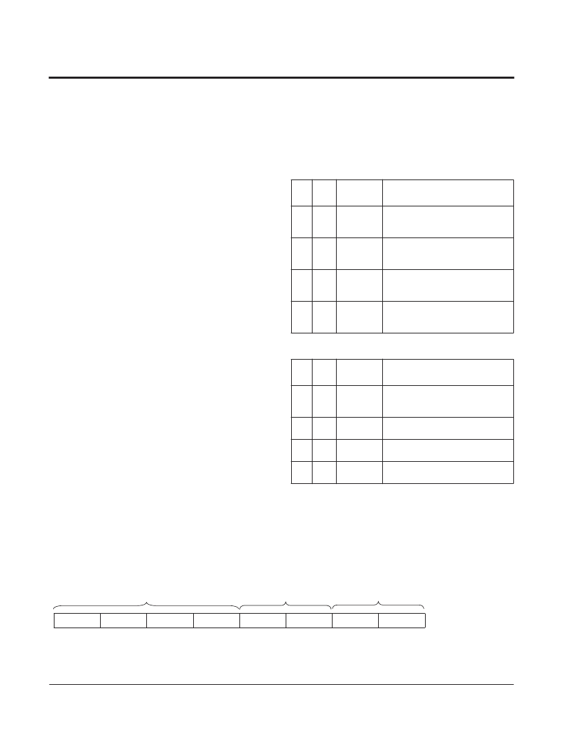
Register Selection (DR0 to DR3) Table
Register Bank Selection (Bank 0 to Bank 3) Table
RB
0
RA
0
Register
Selection
0
Operations
Data Register Read and Write;
Wiper Counter Register
Operations
Data Register Read and Write;
Wiper Counter Register
Operations
Data Register Read and Write;
Wiper Counter Register
Operations
Data Register Read and Write;
Wiper Counter Register
Operations
0
1
1
1
0
2
1
1
3
P1
0
P0
0
Bank
Selection
0
Operations
Data Register Read and Write;
Wiper Counter Register
Operations
Data Register Read and Write
Only
Data Register Read and Write
Only
Data Register Read and Write
Only
0
1
1
1
0
2
1
1
3
Table 4. Identification Byte Format
ID3
0
(MSB)
ID2
1
ID1
0
ID0
1
0
0
A1
A0
(LSB)
Device Type
Identifier
Set to 0
for proper operation
Internal
Slave Address
相關(guān)PDF資料 |
PDF描述 |
|---|---|
| X9271TVI-2.7 | Single Digitally-Controlled (XDCP) Potentiometer |
| X9271UB | Single Digitally-Controlled (XDCP) Potentiometer |
| X9271UB-2.7 | Single Digitally-Controlled (XDCP) Potentiometer |
| X9271UBI | Single Digitally-Controlled (XDCP) Potentiometer |
| X9271UV | Single Digitally-Controlled (XDCP) Potentiometer |
相關(guān)代理商/技術(shù)參數(shù) |
參數(shù)描述 |
|---|---|
| X9271TVI-2.7 | 制造商:INTERSIL 制造商全稱:Intersil Corporation 功能描述:Single Supply/Low Power/256-Tap/SPI Bus |
| X9271TXXX | 制造商:未知廠家 制造商全稱:未知廠家 功能描述:DIGITAL POTENTIOMETER|CMOS|BGA|PLASTIC |
| X9271TXXX-2.7 | 制造商:未知廠家 制造商全稱:未知廠家 功能描述:DIGITAL POTENTIOMETER|CMOS|BGA|PLASTIC |
| X9271TXXXI | 制造商:未知廠家 制造商全稱:未知廠家 功能描述:DIGITAL POTENTIOMETER|CMOS|BGA|PLASTIC |
| X9271TXXXI-2.7 | 制造商:未知廠家 制造商全稱:未知廠家 功能描述:DIGITAL POTENTIOMETER|CMOS|BGA|PLASTIC |
發(fā)布緊急采購,3分鐘左右您將得到回復(fù)。