- 您現(xiàn)在的位置:買賣IC網(wǎng) > PDF目錄371251 > X4003 (Intersil Corporation) Thyristor Diode Module; Repetitive Reverse Voltage Max, Vrrm:1200V; Current Rating:220A PDF資料下載
參數(shù)資料
| 型號(hào): | X4003 |
| 廠商: | Intersil Corporation |
| 英文描述: | Thyristor Diode Module; Repetitive Reverse Voltage Max, Vrrm:1200V; Current Rating:220A |
| 中文描述: | CPU監(jiān)控 |
| 文件頁數(shù): | 8/18頁 |
| 文件大小: | 378K |
| 代理商: | X4003 |
X4003/X4005
Characteristics subject to change without notice.
8 of 18
REV 1.1.3 4/30/02
www.xicor.com
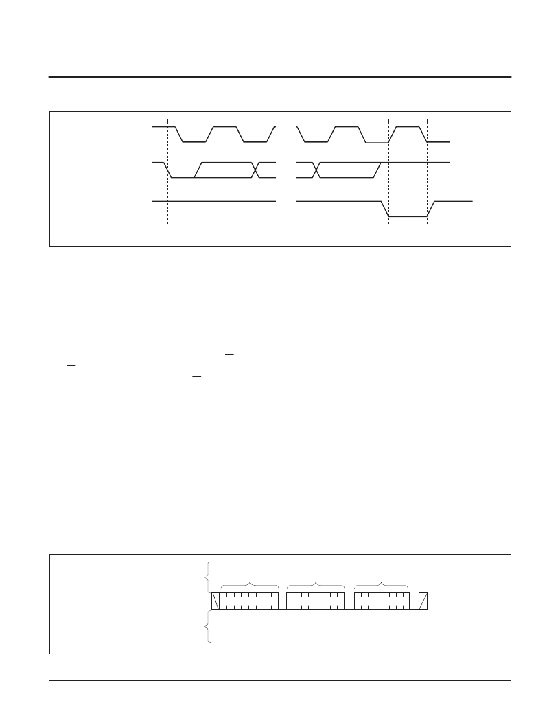
Figure 7. Acknowledge Response From Receiver
Data Output
from Transmitter
Data Output
from Receiver
8
1
9
Start
Acknowledge
SCL from
Master
SERIAL WRITE OPERATIONS
Slave Address Byte
Following a start condition, the master must output a
slave address byte. This byte consists of several parts:
– a device type identifier that is always ‘1011’.
– two bits of ‘0’.
– one bit of the slave command byte is a R/W bit. The
R/W bit of the slave address byte defines the opera-
tion to be performed. When the R/W bit is a one, then
a read operation is selected. A zero selects a write
operation. Refer to Figure 8.
– After loading the entire slave address byte from the
SDA bus, the device compares the input slave byte
data to the proper slave byte. Upon a correct com-
pare, the device outputs an acknowledge on the SDA
line.
Write Control Register
To write to the control register, the device requires the
slave address byte and a byte address. This gives the
master access to register. After receipt of the address
byte, the device responds with an acknowledge, and
awaits the data. After receiving the 8 bits of the data
byte, the device again responds with an acknowledge.
The master then terminates the transfer by generating
a stop condition, at which time the device begins the
internal write cycle to the nonvolatile memory. During
this internal write cycle, the device inputs are disabled,
so the device will not respond to any requests from the
master. If WP is HIGH, the control register cannot be
changed. A write to the control register will suppress
the acknowledge bit and no data in the control register
will change. With WP low, a second byte written to the
control register terminates the operation and no write
occurs.
Stops and Write Modes
Stop conditions that terminate write operations must
be sent by the master after sending 1 full data byte
plus the subsequent ACK signal. If a stop is issued in
the middle of a data byte, or before 1 full data byte plus
its associated ACK is sent, then the device will reset
itself without performing the write.
Figure 8. Write Control Register Sequence
0
Slave
Address
Byte
Address
Data
A
C
K
A
C
K
A
C
K
SDA Bus
Signals from
the Slave
Signals from
the Master
S
S
1
0
0
1
1
0
1
1
1
1
1
1
1
1
1
相關(guān)PDF資料 |
PDF描述 |
|---|---|
| X4003S8I | SCR Thyristor; SCR Type:Standard Gate; Peak Repetitive Off-State Voltage, Vdrm:1600V; On-State RMS Current, IT(rms):24A; Peak Non Repetitive Surge Current, Itsm:450A; Gate Trigger Current Max, Igt:100mA |
| X4003S8I-2.7 | THYRISTOR, 450A, 1220V, B-8; Thyristor/Triac type:Thyristor; Voltage, Vdrm:1200V; Current, It rms:700A; Current, Itsm:5700A; Current, Igt:150mA; Voltage, Vgt:1.65V; Case style:B8; Current, It av:340A; Diameter, External:41mm; Length RoHS Compliant: Yes |
| X4003S8I-2.7A | ; Peak Reflow Compatible (260 C):Yes |
| X4003S8I-4.5A | SCR Thyristor; SCR Type:Standard Gate; Peak Repetitive Off-State Voltage, Vdrm:1600V; On-State RMS Current, IT(rms):38A; Peak Non Repetitive Surge Current, Itsm:700A; Gate Trigger Current Max, Igt:150mA |
| X4005M8I | RTC Module With CPU Supervisor |
相關(guān)代理商/技術(shù)參數(shù) |
參數(shù)描述 |
|---|---|
| X4003_06 | 制造商:INTERSIL 制造商全稱:Intersil Corporation 功能描述:CPU Supervisor |
| X40030 | 制造商:INTERSIL 制造商全稱:Intersil Corporation 功能描述:Triple Voltage Monitor with Intergrated CPU Supervisor |
| X40030_06 | 制造商:INTERSIL 制造商全稱:Intersil Corporation 功能描述:Triple Voltage Monitor with Integrated CPU Supervisor |
| X40030_13 | 制造商:INTERSIL 制造商全稱:Intersil Corporation 功能描述:Triple Voltage Monitor with Integrated CPU Supervisor |
| X40030A | 制造商:INTERSIL 制造商全稱:Intersil Corporation 功能描述:Triple Voltage Monitor with Integrated CPU Supervisor |
發(fā)布緊急采購(gòu),3分鐘左右您將得到回復(fù)。