- 您現(xiàn)在的位置:買賣IC網(wǎng) > PDF目錄371194 > X20C17P-35 CAT5 SHLD, PVC PATCH CBL STRGHT PIN, 100 MHZ-RED PDF資料下載
參數(shù)資料
| 型號: | X20C17P-35 |
| 英文描述: | CAT5 SHLD, PVC PATCH CBL STRGHT PIN, 100 MHZ-RED |
| 中文描述: | 高速自動存儲⑩NOVRAM |
| 文件頁數(shù): | 3/11頁 |
| 文件大小: | 47K |
| 代理商: | X20C17P-35 |
X20C17
3
DEVICE OPERATION
The
CE
,
OE
, and
WE
inputs control the X20C17 opera-
tion. The X20C17 byte-wide NOVRAM uses a
2-line control architecture to eliminate bus contention in
a system environment. The I/O bus will be in a high
impedance state when either
OE
or
CE
is HIGH.
RAM Operations
RAM read and write operations are performed as they
would be with any static RAM. A read operation requires
CE
and
OE
to be LOW. A write operation requires
CE
and
WE
to be LOW. There is no limit to the number of
read or write operations performed to the RAM portion
of the X20C17.
Memory Transfer Operations
There are two memory transfer operations: a recall
operation whereby the data stored in the E
2
PROM array
is transferred to the RAM array; and a store operation
which causes the entire contents of the RAM array to be
stored in the E
2
PROM array.
Recall operations are performed automatically upon
power-up.
Store operations are performed automatically upon
power-down. The store operation take a maximum of
2.5ms.
Write Protection
The X20C17 supports two methods of protecting the
nonvolatile data.
—If after power-up no RAM write operations have
occured, no AUTOSTORE operation can be initiated.
—V
CC
Sense – All functions are inhibited when V
CC
is
≤
3V typical.
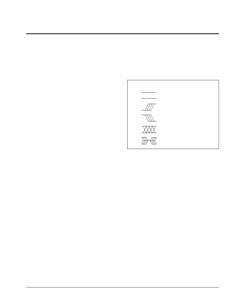
SYMBOL TABLE
The following symbol table provides a key to under-
standing the conventions used in the device timing
diagrams. The diagrams should be used in conjunction
with the device timing specifications to determine actual
device operation and performance, as well as device
suitability for user’s application.
WAVEFORM
INPUTS
OUTPUTS
Must be
steady
Will be
steady
May change
from LOW
to HIGH
Will change
from LOW
to HIGH
May change
from HIGH
to LOW
Will change
from HIGH
to LOW
Don’t Care:
Changes
Allowed
N/A
Changing:
State Not
Known
Center Line
is High
Impedance
相關(guān)PDF資料 |
PDF描述 |
|---|---|
| X20C17P-45 | CAT5 SHLD, PVC PATCH CBL STRGHT PIN, 100 MHZ-RED |
| X20C17P-55 | GIGATRUE 550 CAT6 PATCH 1 FT, SNAGLESS, GRAY |
| X20C17PM-55 | LOCKNUT, ZINC-PLATED, 1" RoHS Compliant: Yes |
| X2111PHT | Analog IC |
| X2111PLT | 55V Single N-Channel HEXFET Power MOSFET in a TO-247AC package; A IRFP1405 with Standard Packaging |
相關(guān)代理商/技術(shù)參數(shù) |
參數(shù)描述 |
|---|---|
| X20C17P-45 | 制造商:XICOR 制造商全稱:Xicor Inc. 功能描述:High Speed AUTOSTORE⑩ NOVRAM |
| X20C17P-55 | 制造商:XICOR 制造商全稱:Xicor Inc. 功能描述:High Speed AUTOSTORE⑩ NOVRAM |
| X20C17PI-35 | 制造商:XICOR 制造商全稱:Xicor Inc. 功能描述:High Speed AUTOSTORE⑩ NOVRAM |
| X20C17PI-45 | 制造商:XICOR 制造商全稱:Xicor Inc. 功能描述:High Speed AUTOSTORE⑩ NOVRAM |
| X20C17PI-55 | 制造商:XICOR 制造商全稱:Xicor Inc. 功能描述:High Speed AUTOSTORE⑩ NOVRAM |
發(fā)布緊急采購,3分鐘左右您將得到回復(fù)。