- 您現(xiàn)在的位置:買賣IC網(wǎng) > PDF目錄231502 > WMF512K8-120CM5A (MICROSEMI CORP-PMG MICROELECTRONICS) 512K X 8 FLASH 5V PROM, 120 ns, CDIP32 PDF資料下載
參數(shù)資料
| 型號: | WMF512K8-120CM5A |
| 廠商: | MICROSEMI CORP-PMG MICROELECTRONICS |
| 元件分類: | PROM |
| 英文描述: | 512K X 8 FLASH 5V PROM, 120 ns, CDIP32 |
| 封裝: | 0.600 INCH, HERMETIC SEALED, SINGLE CAVITY, CERAMIC, SDIP-32 |
| 文件頁數(shù): | 11/13頁 |
| 文件大小: | 375K |
| 代理商: | WMF512K8-120CM5A |
7
White Electronic Designs Corporation (602) 437-1520 www.whiteedc.com
White Electronic Designs
WMF512K8-XXX5
November 2005
Rev. 6
White Electronic Designs Corp. reserves the right to change products or specications without notice.
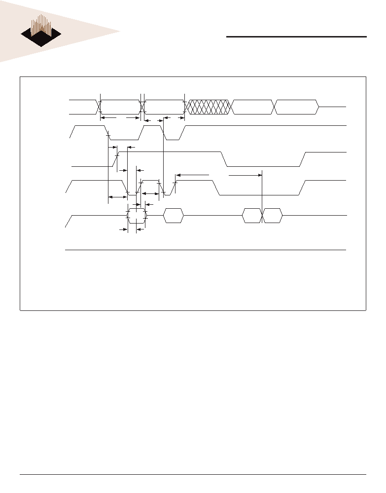
Notes:
1. PA represents the address of the memory location to be programmed.
2. PD represents the data to be programmed at byte address.
3. I/O7# is the output of the complement of the data written to the device.
4. I/OOUT is the output of the data written to the device.
5. Figure indicates the last two bus cycles of a four bus cycle sequence.
Addresses
WE#
OE#
CS#
Data
5.0 V
5555H
PA
tWC
tWS
PD
I/O7#
I/OOUT
tAH
tCPH
tCP
tDH
tDS
Data# Polling
tAS
tGHEL
A0H
tWHWH1
ALTERNATE CS# CONTROLLED PROGRAMMING OPERATION TIMINGS
發(fā)布緊急采購,3分鐘左右您將得到回復(fù)。