- 您現(xiàn)在的位置:買賣IC網(wǎng) > PDF目錄202139 > WED3EL7216S7ES (MICROSEMI CORP-PMG MICROELECTRONICS) 16M X 72 DDR DRAM, 0.75 ns, PBGA219 PDF資料下載
參數(shù)資料
| 型號(hào): | WED3EL7216S7ES |
| 廠商: | MICROSEMI CORP-PMG MICROELECTRONICS |
| 元件分類: | DRAM |
| 英文描述: | 16M X 72 DDR DRAM, 0.75 ns, PBGA219 |
| 封裝: | BGA-219 |
| 文件頁(yè)數(shù): | 3/12頁(yè) |
| 文件大小: | 1001K |
| 代理商: | WED3EL7216S7ES |
11
White Electronic Designs Corporation (602) 437-1520 www.whiteedc.com
WED3EL7216S
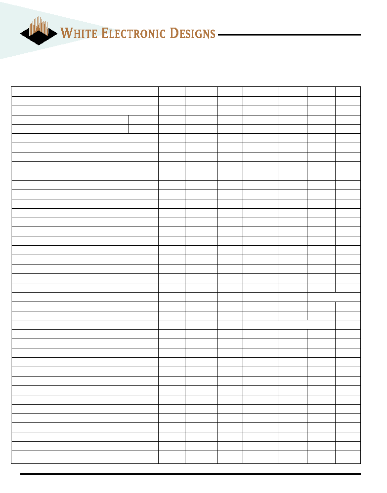
Parameter
Symbol
7
75
8
Access window of DQs from CLKx / CLKx\
tAC
-0.75
0.75
-0.75
0.75
-0.80
0.80
CLKx high level width
tCH
0.45
0.55
0.45
0.55
0.45
0.55
CLKx low level width
tCL
0.45
0.55
0.45
0.55
0.45
0.55
Clock Cycle Time
tCK
7.50
13.00
7.50
13.00
8.00
13.00
tCK
7.50
13.00
10.00
13.00
10.00
13.00
DQ and DM input hold time relative to DQS
tDH
0.50
0.60
DQ and DM input setup time relative to DQS
tDS
0.50
0.60
DQ and DM input pulse width
tDIPW
1.75
2.00
Access window of DQS frm CLKx / CLKx\
tDQSCK
-0.75
0.75
-0.75
0.75
-0.80
0.80
DQS input high pulse width
tDQSH
0.35
DQS input low pulse width
tDQSL
0.35
DQS-DQ skew, DQS to last DQ valid, per group, per access
tDQSQ
0.50
0.60
Wrtie command to first DQS latching transition
tDQSS
0.75
1.25
0.75
1.25
0.75
1.25
DQS falling edge to CLKx rising - setup time
tDSS
0.20
DQS falling edge to CLKX rising - hold time
tDSH
0.20
Half clock period
tHP
tCH,tCL
Data-out high impedance window from CLK/CLK\
tHZ
0.75
0.80
Data-out low impedance window from CLK/CLK\
tLZ
-0.75
-0.80
Address and control input hold time
tIH
0.90
1.10
Address and control input setup time
tIS
1.00
1.10
Load Mode Register
tMRD
15.00
16.00
DQ-DQS hold, DQS to first DQ to go non-valid
tQH
tHP - tQHS
Data hold skew factor
tQHS
0.75
1.00
ACTIVE to PRECHARGE command
tRAS
40.00
120K
40.00
120K
40.00
120K
ACTIVE to READ with AUTO PRECHARGE command
tRAP
tRAS (min) - (burst length x tCLK/e)
ACTIVE to ACTIVE/AUTO REFRESH command period
tRC
65.00
70.00
AUTO REFRESH command period
tRFC
75.00
80.00
ACTIVE to READ or WRITE
tRCD
20.00
PRECHARGE command period
tRP
20.00
DQS read preamble
tRPRE
0.90
1.10
0.90
1.10
0.90
1.10
DQS read postamble
tRPST
0.40
0.60
0.40
0.60
0.40
0.60
ACTIVE bank to ACTIVE bank b command
tRRD
15.00
DQS write preamble
tWPRE
0.25
DQS write preamble setup time
tWPRES
0.00
Half clock period
tWPST
0.40
0.60
0.40
0.60
0.40
0.60
Data-out high impedance window from CLK/CLK\
tWR
15.00
Data-out low impedance window from CLK/CLK\
tREFC
140.60
Address and control input hold time
tXSNR
75.00
80.00
Address and control input setup time
tXSRD
200.00
AC ELECTRICAL CHARACTERISTICS
CL=2.5
CL = 2
相關(guān)PDF資料 |
PDF描述 |
|---|---|
| WF128K32-150G2C5A | 128K X 32 FLASH 5V PROM MODULE, 150 ns, CQFP68 |
| WF128K32-150G2I5 | 128K X 32 FLASH 5V PROM MODULE, 150 ns, CQFP68 |
| WV3HG264M72EEU403D7MG | 128M X 72 DDR DRAM MODULE, 0.6 ns, DMA244 |
| WEDPS512K32-15BM | 512K X 32 MULTI DEVICE SRAM MODULE, 15 ns, PBGA143 |
| WPF1024K32-90PBC | 4M X 8 FLASH 12V PROM MODULE, 90 ns, PBGA84 |
相關(guān)代理商/技術(shù)參數(shù) |
參數(shù)描述 |
|---|---|
| WED416S16030A | 制造商:WEDC 制造商全稱:White Electronic Designs Corporation 功能描述:4M x 16 Bits x 4 Banks Synchronous DRAM |
| WED416S16030C10SI | 制造商:WEDC 制造商全稱:White Electronic Designs Corporation 功能描述:4M x 16 Bits x 4 Banks Synchronous DRAM |
| WED416S16030C75SI | 制造商:WEDC 制造商全稱:White Electronic Designs Corporation 功能描述:4M x 16 Bits x 4 Banks Synchronous DRAM |
| WED416S16030C7SI | 制造商:WEDC 制造商全稱:White Electronic Designs Corporation 功能描述:4M x 16 Bits x 4 Banks Synchronous DRAM |
| WED416S16030C8SI | 制造商:WEDC 制造商全稱:White Electronic Designs Corporation 功能描述:4M x 16 Bits x 4 Banks Synchronous DRAM |
發(fā)布緊急采購(gòu),3分鐘左右您將得到回復(fù)。