- 您現(xiàn)在的位置:買賣IC網(wǎng) > PDF目錄202119 > W7NCF256H20IS3AG (WHITE ELECTRONIC DESIGNS CORP) 16M X 16 FLASH 3.3V PROM CARD, 150 ns, UUC PDF資料下載
參數(shù)資料
| 型號(hào): | W7NCF256H20IS3AG |
| 廠商: | WHITE ELECTRONIC DESIGNS CORP |
| 元件分類: | PROM |
| 英文描述: | 16M X 16 FLASH 3.3V PROM CARD, 150 ns, UUC |
| 封裝: | CARD |
| 文件頁(yè)數(shù): | 10/13頁(yè) |
| 文件大小: | 172K |
| 代理商: | W7NCF256H20IS3AG |
第1頁(yè)第2頁(yè)第3頁(yè)第4頁(yè)第5頁(yè)第6頁(yè)第7頁(yè)第8頁(yè)第9頁(yè)當(dāng)前第10頁(yè)第11頁(yè)第12頁(yè)第13頁(yè)
March 2007
Rev. 10
W7NCFxxx-H Series
6
White Electronic Designs Corporation (602) 437-1520 www.whiteedc.com
White Electronic Designs
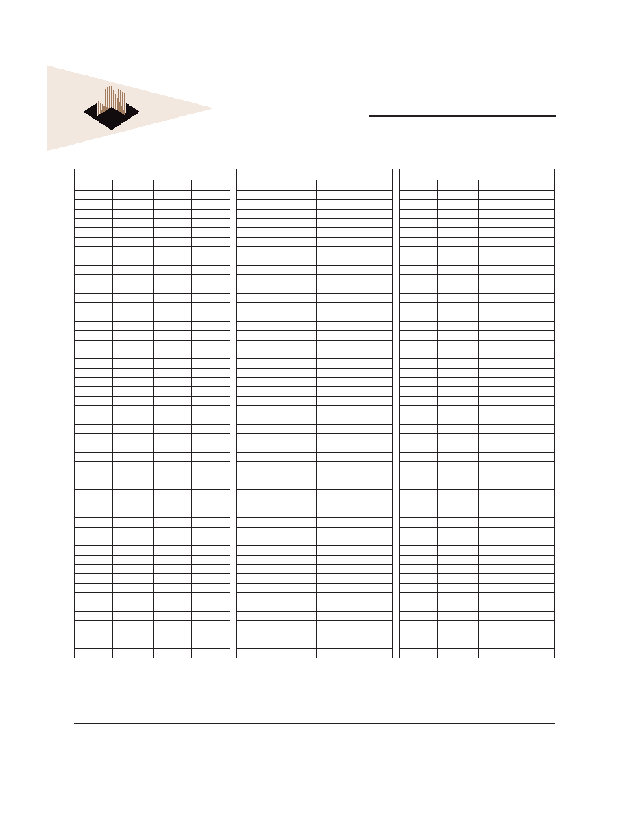
Pin Assignments & Pin Type
PC Card Memory Mode
Pin Number Signal Name
Pin Type
In, Out Type
1
GND
Ground
2
D03
I/O
I1Z, OZ3
3
D04
I/O
I1Z, OZ3
4
D05
I/O
I1Z, OZ3
5
D06
I/O
I1Z, OZ3
6
D07
I/O
I1Z, OZ3
7
-CE1
I
I3U
8
A10
I
IZ1
9
-OE
I
IU3
10
A09
I
I1Z
11
A08
I
I1Z
12
A07
I
I1Z
13
VCC
Power
14
A06
I
I1Z
15
A05
I
I1Z
16
A04
I
I1Z
17
A03
I
I1Z
18
A02
I
I1Z
19
A01
I
I1Z
20
A00
I
I1Z
21
D00
I/O
I1Z, OZ3
22
D01
I/O
I1Z, OZ3
23
D02
I/O
I1Z, OZ3
24
WP
O
OT3
25
-CD2
O
Ground
26
-CD1
O
Ground
27
D111
I/O
I1Z, OZ3
28
D121
I/O
I1Z, OZ3
29
D131
I/O
I1Z, OZ3
30
D141
I/O
I1Z, OZ3
31
D151
I/O
I1Z, OZ3
32
-CE21
I
I3U
33
-VS1
O
Ground
34
-IORD
I
I3U
35
-IOWR
I
I3U
36
-WE
I
I3U
37
RDY
O
OT1
38
VCC
Power
39
-CSEL4
I
I2Z
40
-VS2
O
OPEN
41
RESET
I
I2Z
42
-WAIT
O
OT1
43
-INPACK
O
OT1
44
-REG
I
I3U
45
BVD2
O
OT1
46
BVD1
O
OT1
47
DO81
I/O
I1Z, OZ3
48
DO91
I/O
I1Z, OZ3
49
D101
I/O
I1Z, OZ3
50
GND
Ground
PC Card I/O Mode
Pin Number Signal Name
Pin Type
In, Out Type
1
GND
Ground
2
D03
I/O
I1Z, OZ3
3
D04
I/O
I1Z, OZ3
4
D05
I/O
I1Z, OZ3
5
D06
I/O
I1Z, OZ3
6
D07
I/O
I1Z, OZ3
7
-CE1
I
I3U
8
A10
I
IZ1
9
-OE
I
IU3
10
A09
I
I1Z
11
A08
I
I1Z
12
A07
I
I1Z
13
VCC
Power
14
A06
I
I1Z
15
A05
I
I1Z
16
A04
I
I1Z
17
A03
I
I1Z
18
A02
I
I1Z
19
A01
I
I1Z
20
A00
I
I1Z
21
D00
I/O
I1Z, OZ3
22
D01
I/O
I1Z, OZ3
23
D02
I/O
I1Z, OZ3
24
-IOIS16
O
OT3
25
-CD2
O
Ground
26
-CD1
O
Ground
27
D111
I/O
I1Z, OZ3
28
D121
I/O
I1Z, OZ3
29
D131
I/O
I1Z, OZ3
30
D141
I/O
I1Z, OZ3
31
D151
I/O
I1Z, OZ3
32
-CE21
I
I3U
33
-VS1
O
Ground
34
-IORD
I
I3U
35
-IOWR
I
I3U
36
-WE
I
I3U
37
IREQ
O
OT1
38
VCC
Power
39
-CSEL4
I
I2Z
40
-VS2
O
OPEN
41
RESET
I
I2Z
42
-WAIT
O
OT1
43
-INPACK
O
OT1
44
-REG
I
I3U
45
-SPKR
I/O
OT1
46
-STSCHG
I/O
OT1
47
DO81
I/O
I1Z, OZ3
48
DO91
I/O
I1Z, OZ3
49
D101
I/O
I1Z, OZ3
50
GND
Ground
True IDE Mode
Pin Number Signal Name
Pin Type
In, Out Type
1
GND
Ground
2
D03
I/O
I1Z, OZ3
3
D04
I/O
I1Z, OZ3
4
D05
I/O
I1Z, OZ3
5
D06
I/O
I1Z, OZ3
6
D07
I/O
I1Z, OZ3
7
-CS0
I
I3U
8
A102
I
IZ1
9
-ATA SEL
I
IU3
10
A092
I
I1Z
11
A082
I
I1Z
12
A072
I
I1Z
13
VCC
Power
14
A062
I
I1Z
15
A052
I
I1Z
16
A042
I
I1Z
17
A032
I
I1Z
18
A02
I
I1Z
19
A01
I
I1Z
20
A00
I
I1Z
21
D00
I/O
I1Z, OZ3
22
D01
I/O
I1Z, OZ3
23
D02
I/O
I1Z, OZ3
24
-IOIS16
O
ON3
25
-CD2
O
Ground
26
-CD1
O
Ground
27
D111
I/O
I1Z, OZ3
28
D121
I/O
I1Z, OZ3
29
D131
I/O
I1Z, OZ3
30
D141
I/O
I1Z, OZ3
31
D151
I/O
I1Z, OZ3
32
-CS11
I
I3Z
33
-VS1
O
Ground
34
-IORD
I
I3Z
35
-IOWR
I
I3Z
36
-WE3
I
I3U
37
IREQ
O
OZ1
38
VCC
Power
39
-CSEL
I
I2U
40
-VS2
O
OPEN
41
RESET
I
I2Z
42
-IORDY
O
ON1
43
DMARQ
O
OZ1
44
-DMACK5
I
I3U
45
-DASP
I/O
I1U, ON1
46
PDIAG
I/O
I1U, ON1
47
DO81
I/O
I1Z, OZ3
48
DO91
I/O
I1Z, OZ3
49
D101
I/O
I1Z, OZ3
50
GND
Ground
Note: 1 These signals are required only for 16-bit access and are not required when
installed in 8-bit systems. Devices should allow for 3-state signals not to
consume current.
2
: Should be grounded by the host system.
3
: Should be tied to VCC by the host system.
4
: The -CSEL signal is ignored by the card in PC Card moudes. However,
because it is not pulled up on the card in thses modes, it should not be left
oating by the host in PC card modes. In these modes, the pin should be
connected by th host to PC card A25 or grounded by the host.
5
: If DMA operations are not used, the signal should be held high or tied to VCC
by the host. For proper operation in older hosts: while DMA operations are not
active, the card shall ignore the signal, including a oating condition.
相關(guān)PDF資料 |
PDF描述 |
|---|---|
| W7NCF256H20IS3FG | 16M X 16 FLASH 3.3V PROM CARD, 150 ns, UUC |
| W7NCF256H20IS3JG | 16M X 16 FLASH 3.3V PROM CARD, 150 ns, UUC |
| W7NCF512H31IS7CG | 32M X 16 FLASH 3.3V PROM CARD, 150 ns, UUC |
| W7NCF512H31ISBBG | 32M X 16 FLASH 3.3V PROM CARD, 150 ns, UUC |
| W3EG72125S202AJD3SG | 128M X 72 DDR DRAM MODULE, 0.8 ns, DMA184 |
相關(guān)代理商/技術(shù)參數(shù) |
參數(shù)描述 |
|---|---|
| W7PCX-1 | 制造商:Magnecraft 功能描述:7PC Series Subminiature 2 A SPDT 5 VDC PCB Through Hole Switching Relay 制造商:Magnecraft 功能描述:Electromechanical Relay SPDT 2A 5VDC 75Ohm Through Hole |
| W7PCX-1/MMS105 | 制造商:Magnecraft 功能描述:Relay;E-Mech;Power;SPDT;Cur-Rtg 2A;Ctrl-V 5DC;Vol-Rtg 120/24AC/DC;PCB Mnt;5 Pin |
| W7PCX-3 | 制造商:Magnecraft 功能描述:Power Relay 制造商:Magnecraft 功能描述:Electromechanical Relay SPDT 2A 12VDC 440Ohm Through Hole |
| W7PCX-4 | 制造商:Magnecraft 功能描述:Electromechanical Relay SPDT 2A 24VDC 1.55KOhm Through Hole |
| W7PCX5 | 制造商:TE Magnecraft 功能描述:Relay 5 vdc DPDT |
發(fā)布緊急采購(gòu),3分鐘左右您將得到回復(fù)。