- 您現在的位置:買賣IC網 > PDF目錄359452 > VV6444C001 (意法半導體) Low Cost Digital Camera (LCDC) Chipset PDF資料下載
參數資料
| 型號: | VV6444C001 |
| 廠商: | 意法半導體 |
| 英文描述: | Low Cost Digital Camera (LCDC) Chipset |
| 中文描述: | 低成本數碼相機(LCDC)芯片組 |
| 文件頁數: | 18/60頁 |
| 文件大小: | 352K |
| 代理商: | VV6444C001 |
第1頁第2頁第3頁第4頁第5頁第6頁第7頁第8頁第9頁第10頁第11頁第12頁第13頁第14頁第15頁第16頁第17頁當前第18頁第19頁第20頁第21頁第22頁第23頁第24頁第25頁第26頁第27頁第28頁第29頁第30頁第31頁第32頁第33頁第34頁第35頁第36頁第37頁第38頁第39頁第40頁第41頁第42頁第43頁第44頁第45頁第46頁第47頁第48頁第49頁第50頁第51頁第52頁第53頁第54頁第55頁第56頁第57頁第58頁第59頁第60頁
PRELIMINARY
Digital Camera Chipset; Customer Datasheet, Rev 3.0, March 2000
STV0680A + VV6444/6410/6500
CDSTV0680F-C
Commercial in confidence
18
T
STV0680F_contents.fm
4.
STV0680A hardware interfaces
4.1
The STV0680A pinout has been carefully developed to minimise the physical size of the support printed circuit board by
facilitating placement of and electrical routing to peripheral support components such as the SDRAM. The complete pinout and
listing is shown in Section 8.
STV0680A pinout
4.2
STV0680A uses a standard ST digital interface from the sensor, and the sensor clock input is provided by an output from
STV0680A. Designing a camera using this chipset should design as close as possible to the reference design (Section 9.), in
which case the chipset can be regarded as a functional ‘black box’, and no further details regarding the STV0680A-sensor
interface are required.
Sensor interface
4.3
STV0680A is designed to interface to an external 16Mbit or 64Mbit SDRAM (see Table 4 and Table 5). The SDRAM device must
have a 16 bit wide data bus and operate from a 3.3V supply. Two sizes of SDRAM memory are supported by STV0680A, 16MBits
(1M x 16 bits wide) or 64MBits (4M x 16 bits wide), the memory size is auto-detected by STV0680A. STV0680A clocks the
SDRAM at 6MHz, typically this is well below the figures offered by most manufacturers’ devices. Devices which are PC66 and/or
PC100 compliant are preferred. For interface wiring, see Section 9.
Memory interface
4.3.1
For maximum system battery life while no pictures are being taken, and to assist in meeting requirements for USB compliance, an
SDRAM should be chosen with the lowest possible self refresh current specification. For suggested SDRAM part numbers, see
Section 9.
SDRAM Current consumption
4.3.2
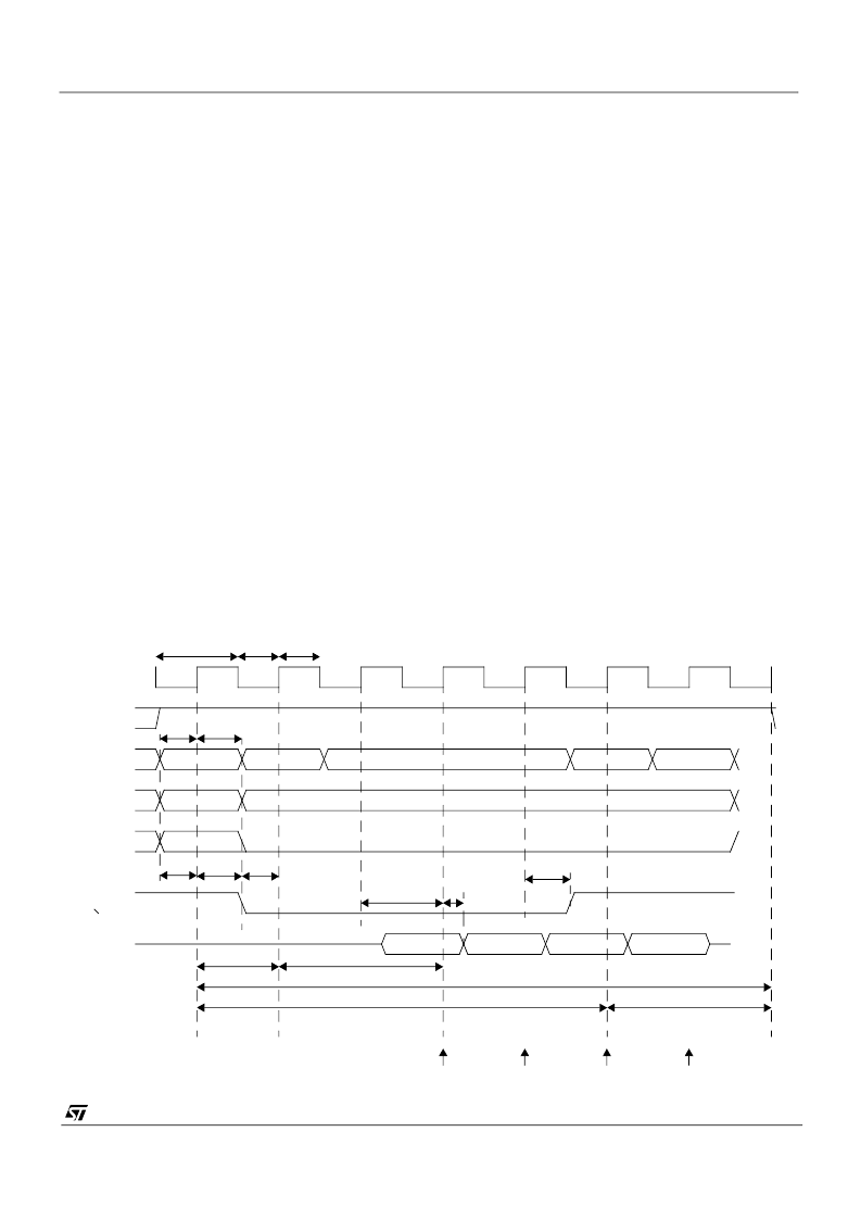
The following timing diagrams should be referred to when selecting SDRAM other than those recommended in Section 9.
SDRAM interface timing requirements
DCLK
Command
DQM
A0-9,BA
A10
ACTIVE
READ
NOP
PRECHARGE
NOP
ROW
COLUMN
ROW
DOUT M
DOUT M + 1
DOUT M + 2
DOUT M + 3
DQ
READ Latency
t
CK
t
RCD
t
RC
CKE
t
RAS
DQ sample
DQ sample
DQ sample
DQ sample
t
RP
t
CMS
t
CMH
t
AS
t
AH
t
L
t
H
t
CMS
t
CMH
t
AC
t
OH
相關PDF資料 |
PDF描述 |
|---|---|
| VV6501C001 | DUAL-MODE DIGITAL CAMERA CO-PROCESSOR |
| VV6501 | DUAL-MODE DIGITAL CAMERA CO-PROCESSOR |
| VVA1 | VVA1, VVA2, VVA3 Full Size VCXO |
| VVB1 | Half Size VCXO |
| VVC1-CNB-35.328 | Voltage Controlled Crystal Oscillator |
相關代理商/技術參數 |
參數描述 |
|---|---|
| VV64498-11E | 制造商:Carling Technologies 功能描述:V-SERIES ROCKER SWITCH - Bulk |
| VV64800-000 | 制造商:Carling Technologies 功能描述:V-SERIES ROCKER SWITCH - Bulk |
| VV64R00-000 | 制造商:Carling Technologies 功能描述:V-SERIES ROCKER SWITCH - Bulk |
| VV64Z00-000 | 制造商:Carling Technologies 功能描述:V-SERIES ROCKER SWITCH - Bulk |
| VV64Z13-000 | 制造商:Carling Technologies 功能描述:V-SERIES ROCKER SWITCH - Bulk |
發(fā)布緊急采購,3分鐘左右您將得到回復。