- 您現(xiàn)在的位置:買賣IC網(wǎng) > PDF目錄359432 > VSC880 (VITESSE SEMICONDUCTOR CORP) High Performance 16x16 Serial Crosspoint Switch PDF資料下載
參數(shù)資料
| 型號: | VSC880 |
| 廠商: | VITESSE SEMICONDUCTOR CORP |
| 元件分類: | 路由/交換 |
| 英文描述: | High Performance 16x16 Serial Crosspoint Switch |
| 中文描述: | TELECOM, DIGITAL TIME SWITCH, PBGA304 |
| 封裝: | BGA-304 |
| 文件頁數(shù): | 4/28頁 |
| 文件大小: | 390K |
| 代理商: | VSC880 |
第1頁第2頁第3頁當(dāng)前第4頁第5頁第6頁第7頁第8頁第9頁第10頁第11頁第12頁第13頁第14頁第15頁第16頁第17頁第18頁第19頁第20頁第21頁第22頁第23頁第24頁第25頁第26頁第27頁第28頁
VITESSE
Data Sheet
VSC880
High Performance 16x16
Serial Crosspoint Switch
Page 4
G52191-0, Rev 4.2
01/05/01
VITESSE
SEMICONDUCTOR CORPORATION
741 Calle Plano
Camarillo, CA 93012
Tel: (800) VITESSE
FAX: (805) 987-5896
Email: prodinfo@vitesse.com
Internet: www.vitesse.com
Functional Description
The VSC880 switch can be used in conjunction with the VSC870 transceivers to support two modes of
operation: Packet Mode and Cell Mode. In Packet mode, the chip set provides a switching system to support variable
length, self-routing data packets. In Cell Mode, the chip set provides a cell synchronous switching system with a user
defined scheduler. In this mode, it can support only fixed length data packets (cells). Routing decisions are carried
out in the scheduler and crosspoint configuration is synchronized to a cell clock. The scheduler configures the switch
matrix using the parallel interface. To conserve power, each serial port quadrant can be powered down if not used.
The following section gives a detailed functional description of the operation of the switch chip. Most of the
discussion includes some of the transceiver operation (see the VSC870 data sheet). The two major operation modes
are described separately in the
Packet Mode
and the
Cell Mode
sections.
1.0 Common Features
1.1 Synchronization
1.1.1 Link Characteristic
The serial link is used to connect the switch chip to transceivers. These links operate at 2.125 Gb/s and are
initialized simultaneously at power up, or separately when a link error occurs. A link is first bit synchronized, then
word synchronized and, if CMODE is HIGH, cell synchronized. In Packet or Cell mode, the switch acts as the
master, generating the bit clock along with the word and cell boundary information. The transceivers act as slaves,
recovering the bit clock, word clock and cell clock. The transceiver also contains redundant serial inputs and outputs
which can be used with a redundant switch chip.
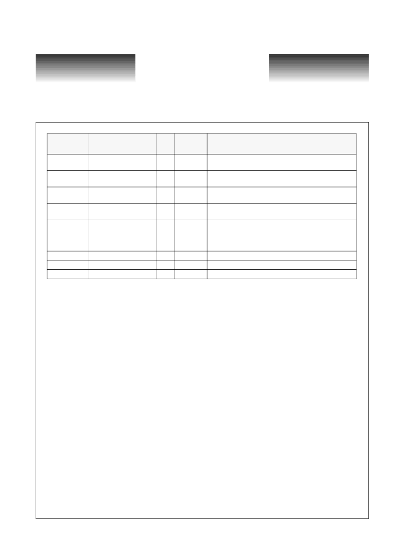
LOCKDET
CMU Lock Detect
O
<1MHz
TTL
<1MHz
TTL
<1MHz
TTL
<1MHz
VECL
This signal is LOW while the CMU is acquiring lock.
VSCTE
NOR Chain Test Enable
I
Used for ATE testing of the parametric NOR chain in the I/O
frame. Set to logic LOW during normal operation.
Used for ATE testing of the parametric NOR chain in the I/O
frame. Set to logic LOW during normal operation.
Used for ATE testing of the parametric NOR chain in the I/O
frame. Leave output open during normal operation.
VDD1 = Serial Port 0-3 power supply
VDD2 = Serial Port 4-7 power supply
VDD3 = Serial Port 8-11 power supply
VDD4 = Serial Port 12-15 power supply
Clean power supply for CMU
Clean ground for CMU
Core power supply
VSCIPNC
NOR Chain Input
I
VSCOPNC
NOR Chain Output
O
VDD1, VDD2,
VDD3, VDD4
Serial Port Power
Supplies
P
3.3V
VDDA
VSSA
VMM
CMU Power Supply
CMU Ground
Core Power Supply
P
P
P
3.3V
0V
2 ~ 2.5V
Pin
Name
I/O
Freq
Type
Description
相關(guān)PDF資料 |
PDF描述 |
|---|---|
| VSC9110 | Target Specification |
| VSC9115 | 2.5 Gb/s Multi-Service SONET/SDH Mapper Device with Virtual Concatenation |
| VSC9118 | 10 Gb/s / Quad 2.5 Gb/s Multi-Service SONET/SDH Mapper Device with Virtual Concatenation |
| VSC9125 | Enhanced 2.5,10 Gbps Multiservice SONET/SDH VC Mapper |
| VSC9135 | Multi-service High Order/Low Order Virtual Concatenation mapper |
相關(guān)代理商/技術(shù)參數(shù) |
參數(shù)描述 |
|---|---|
| VSC880TY | 制造商:VITESSE 制造商全稱:Vitesse Semiconductor Corporation 功能描述:High Performance 16x16 Serial Crosspoint Switch |
| VSC882 | 制造商:VITESSE 制造商全稱:Vitesse Semiconductor Corporation 功能描述:80 Gb/s Intelligent Switch Fabric |
| VSC9110 | 制造商:VITESSE 制造商全稱:Vitesse Semiconductor Corporation 功能描述:Target Specification |
| VSC9115 | 制造商:VITESSE 制造商全稱:Vitesse Semiconductor Corporation 功能描述:2.5 Gb/s Multi-Service SONET/SDH Mapper Device with Virtual Concatenation |
| VSC9118 | 制造商:VITESSE 制造商全稱:Vitesse Semiconductor Corporation 功能描述:10 Gb/s / Quad 2.5 Gb/s Multi-Service SONET/SDH Mapper Device with Virtual Concatenation |
發(fā)布緊急采購,3分鐘左右您將得到回復(fù)。