- 您現(xiàn)在的位置:買賣IC網(wǎng) > PDF目錄358551 > VPLD31TEM-666.5143MHZ (CONNOR WINFIELD CORP) VCXO, CLOCK, 666.5143 MHz, LVPECL OUTPUT PDF資料下載
參數(shù)資料
| 型號(hào): | VPLD31TEM-666.5143MHZ |
| 廠商: | CONNOR WINFIELD CORP |
| 元件分類: | XO, clock |
| 英文描述: | VCXO, CLOCK, 666.5143 MHz, LVPECL OUTPUT |
| 文件頁(yè)數(shù): | 1/2頁(yè) |
| 文件大小: | 211K |
| 代理商: | VPLD31TEM-666.5143MHZ |
THE CONNOR-WINFIELD CORP.
2111 COMPREHENSIVE DRIVE.
AURORA, IL 60505.
FAX (630) 851-5040.
PHONE (630) 851-4722.
HTTP://WWW.CONWIN.COM
P R O D UC T D ATA S HE E T
Specifications subject to change without notice.
Copyright 2001 Connor-Winfield all rights reserved.
DATA SHEET #:
REV:
DATE:
PAGE
OF
a
CRYSTAL CONTROLLED OSCILLATORS
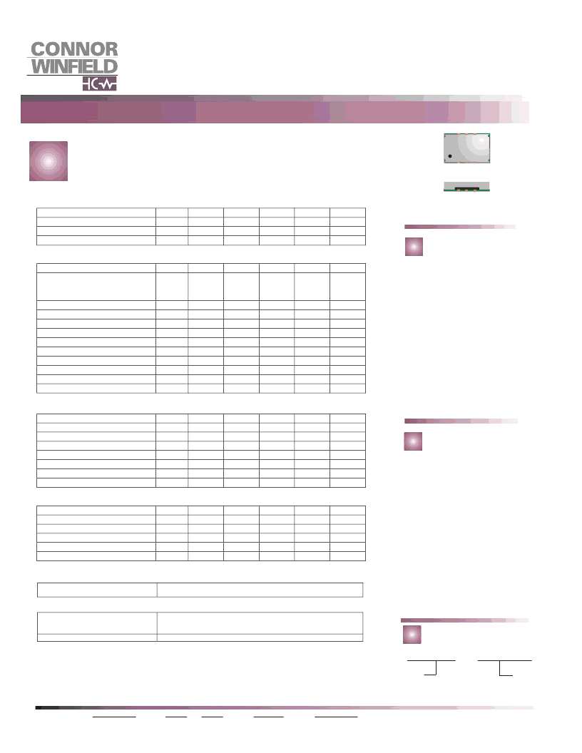
The Connor-Winfield
VPLD31TEM is a 3.3V Voltage
Controlled Crystal Oscillator
(VCXO) with Differential
LVPECL outputs and
Enable/Disable function. The
VPLD31TEM is designed for
use with PLL systems requiring
low jitter and tight stability. No
PLL multiplication schemes are
used in this oscillator design.
1
2
VPLD31TEM - 669.3266MHz
VCXO
SERIES
CENTER
FREQUENCY
FEATURES
DESCRIPTION
ORDERING INFORMATION
LOW PROFILE, SURFACE MOUNT
PACKAGE
3.3V OPERATION
LOW JITTER <1pS RMS
FREQUENCY TOLERANCE: ±25ppm
TEMPERATURE RANGE: 0 to 85°C
DIFFERENTIAL LVPECL OUTPUTS
ENABLE / DISABLE FUNCTION
TAPE AND REEL PACKAGING
3.3V SURFACE MOUNT VCXO OSCILLATOR
VPLD31TEM
Vx530
01
09/20/05
CW 0535
VPLD31TEM
669.3266M
Notes
1.0
2.0
Inclusive of calibration @25°C, frequency vs. temperature, aging (15yrs), supply and load variations, shock, and vibration.
Absolute Pull Range (APR) is the minimum guaranteed pull range of the VCXO under all conditions over lifetime
operation. The APR is referenced to Fo
When oscillator is disabled the true output is in a low state (Vol) and the complementary output is in the high state (VoH)
50 ohm termination into Vcc-2V or Thevein equivalent.
3.0
4.0
ABSOLUTE MAXIMUM RATINGS
PARAMETER
Storage Temperature
Supply Voltage
Control Voltage
OPERATING SPECIFICATIONS
PARAMETER
TABLE 1.0
NOTE
UNITS
(Vcc)
(Vc)
MINIMUM
-40
-0.5
-0.5
NOMINAL MAXIMUM
-
-
-
NOMINAL MAXIMUM
622.08000
644.53125
666.51430
669.32660
-
-
3.3
-
-
-
-60
-90
-130
-135
NOMINAL
1.65
-
-
50K
-
-
-
NOMINAL
-
-
-
50
-
UNITS
°C
Vdc
Vdc
85
7.0
7.0
TABLE 2.0
NOTE
MINIMUM
UNITS
Center Frequency
Total Frequency Tolerance
Operating Temperature Range
Supply Voltage
Supply Current
Jitter (BW=10Hz to 20MHz)
Jitter (BW=12kHz to 80MHz)
SSB Phase Noise at 100Hz offset
SSB Phase Noise at 1KHz offset
SSB Phase Noise at 10KHz offset
SSB Phase Noise at 100KHz offset
INPUT CHARACTERISTICS
PARAMETER
Control Voltage Range
Absolute Pull Range (APR)
Monotonic Linearity
Input Impedance
Modulation Bandwidth (3dB)
Enable Input Voltage (Low)
Disable Input Voltage (High)
LVPECL OUTPUT CHARACTERISTICS
PARAMETER
LOAD
Voltage (High)
(Low)
Duty Cycle at 50% Level
Rise / Fall Time measured @ 20% to 80%
PACKAGE CHARACTERISTICS
Package
(Fo)
(Vcc)
(Icc)
(Vc)
(Vil)
(Vih)
-
-
25
85
3.465
100
5
1
-
-
-
-
MHz
ppm
°C
Vdc
mA
ps rms
ps rms
dBc/Hz
dBc/Hz
dBc/Hz
dBc/Hz
-25
0
3.135
-
-
-
-
-
-
-
1
TABLE 3.0
NOTE
MINIMUM
0.3
+/-25
-10
-
10
-
2.275
MAXIMUM
3.0
-
10
-
-
1.68
-
UNITS
Vdc
ppm
%
Ohm
KHz
Vdc
Vdc
2
3
3
TABLE 4.0
NOTE
MINIMUM
-
2.275
-
45
-
MAXIMUM
50
-
1.68
55
1.0
UNITS
Ohms
Vdc
Vdc
%
nS
4
(Voh)
(Vol)
TABLE 5.0
Non-hermetic package consisting of an FR4 substrate with grounded metal
cover.
PROCESS RECOMMENDATIONS
Solder Reflow
TABLE 6.0
The component solder used internal to this device has a melting point of
221
°
C. The peak temperature inside the device should be less than or
equal to 220
°
C for a maximum of 10 seconds
Ultrasonic cleaning is not recommended.
Wash
相關(guān)PDF資料 |
PDF描述 |
|---|---|
| VPLD31TEM-644.53125MHZ | VCXO, CLOCK, 644.53125 MHz, LVPECL OUTPUT |
| VPLD31TEMG5-622.08000MHZ | VCXO, CLOCK, 622.08 MHz, LVPECL OUTPUT |
| VPLD48J3E-100.00MHZ | VCXO, CLOCK, 100 MHz, LVPECL OUTPUT |
| VPLD54TEM-400.0MHZ | VCXO, CLOCK, 400 MHz, LVPECL OUTPUT |
| VPLD61B-155.52MHZ | VCXO, CLOCK, 155.52 MHz, PECL OUTPUT |
相關(guān)代理商/技術(shù)參數(shù) |
參數(shù)描述 |
|---|---|
| VPLD54J3EG155M52 | 制造商:Connor-Winfield 功能描述: |
| VPLD61J2EG15552MHZ | 制造商:Connor-Winfield 功能描述: |
| VPLN-60 | 制造商:CUI 制造商全稱:CUI INC 功能描述:switching power supply |
| VPLN-60-12 | 制造商:CUI 制造商全稱:CUI INC 功能描述:switching power supply |
| VPLN60-12 | 制造商:CUI 制造商全稱:CUI INC 功能描述:switching power supply |
發(fā)布緊急采購(gòu),3分鐘左右您將得到回復(fù)。